Method and apparatus for electrical commoning of circuits

a technology of electrical commoning and circuit, applied in the direction of printed circuit testing, measurement instrument housing, instruments, etc., can solve the problems of electrical circuits that are not suitable for contact with contact pads, electrical commoning mechanisms that are not functional, and “false open”, so as to reduce manufacturing waste and reduce customer complaints

Active Publication Date: 2006-05-02
TWITTER INC
View PDF12 Cites 1 Cited by
  • Summary
  • Abstract
  • Description
  • Claims
  • Application Information

AI Technical Summary

Benefits of technology

[0019]Therefore, an important objective for manufacturers of substrates is their constant desire to find and detect circuits which are flawed and which contain undesired electrical conditions, to thereby reduce manufacturing waste, reduce customer complaints, and the like.
[0020]The present invention provides a method and apparatus for electrically commoning the electronic circuits supported by a substrate, and to effectively and cost efficiently in a timely manner to determine the existence of undesired electrical conditions associated with the electronic circuits to thereby reduce costs associated with manufacturing waste and customer complaints. Flaws in manufacturing processes which may have caused an occurrence of undesired electrical conditions in the electrical circuits thereby creating flawed electrical circuits not being able to function as expected or desired can be effectively detected at an appropriate early stage of the assembling process.
[0021]The present invention provides a method and apparatus for testing the continuity of electronic circuits and to accommodate requirements to make even smaller electronic devices in attempts to physically decrease the size of substrates thereby increasing the density of the electronic circuits and subsequently placing the pads much closer together compared to electronic circuits used in less dense circuits.

Problems solved by technology

Flaws resulting in manufacturing processes of microcircuit devices can create undesired electrical conditions in electrical circuits contained within such devices resulting in flawed or inoperable electrical circuits wherein the flawed circuits do not function as originally intended and designed.
This causes difficulties in effecting contact of the desired individual circuit contact pads on the surface of the substrate for purposes of detecting undesired electrical conditions in the individual circuits.
Problems exist resulting from the use of known electrical-commoning methods and apparatus for detecting undesired electrical condition of electronic circuits on substrates which could produce “false open” results.
the electrical-commoning mechanism does not making suitable contact with the contact pads;
the electrical-commoning means is not sufficiently locally compliant with the pads resulting in ineffective electrical contact;
the electrical-commoning mechanism does not have a capability to overcome aspects of “self-damage” that may be reflected in the contacts so that a reliable commoning of the contact pads can be effected, for example, the self-damage being caused by contaminants, or the pads having surface inconsistencies, or the electrical-commoning mechanism having surface inconsistencies; and
the electrical-commoning means may deposit an unwanted residual electrically non-conductive material on the surface of the pads and the substrate, such that it may be difficult to remove the residual material from the pads and the substrate after testing is performed.
However, difficulties may arise with the use of such polymeric sheets in that:
the sheet may leave a residual contamination on the surface of the pads and substrate during the test which may be difficult to remove;
the sheet has a capability of being susceptible to physical damage when contacting the pads;
the sheet requires relatively large contact forces to ensure that the polymeric sheet makes sufficient contact with all of the pads and the large forces may result in damage to the substrate and any test fixture; and
the sheet may be insufficient to completely prevent “false opens” because the polymeric sheet does not have sufficient capability for being substantially and completely locally compliant with the contact pads.

Method used


Image

  • Method and apparatus for electrical commoning of circuits
  • Method and apparatus for electrical commoning of circuits
  • Method and apparatus for electrical commoning of circuits

Examples


Embodiment Construction

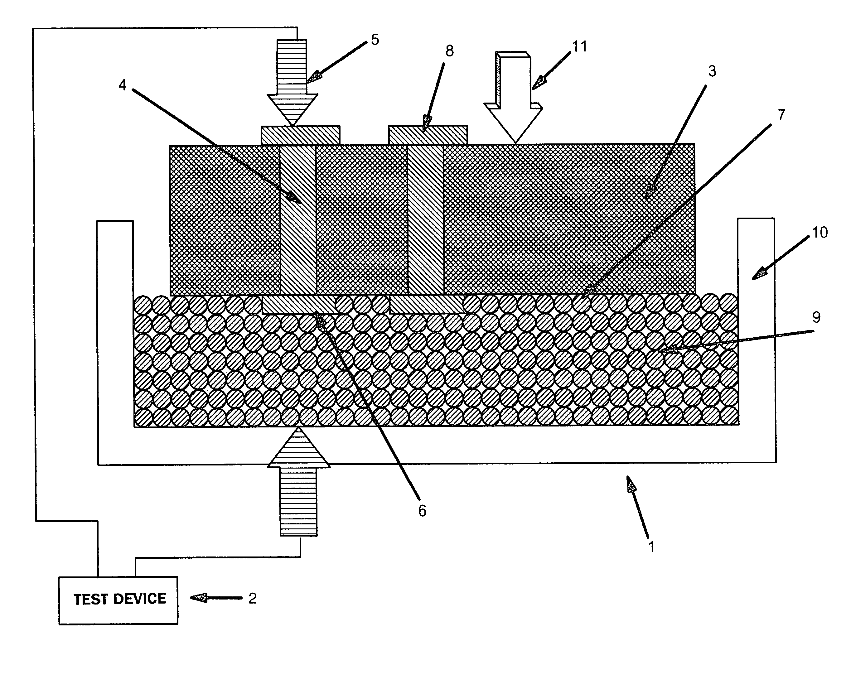
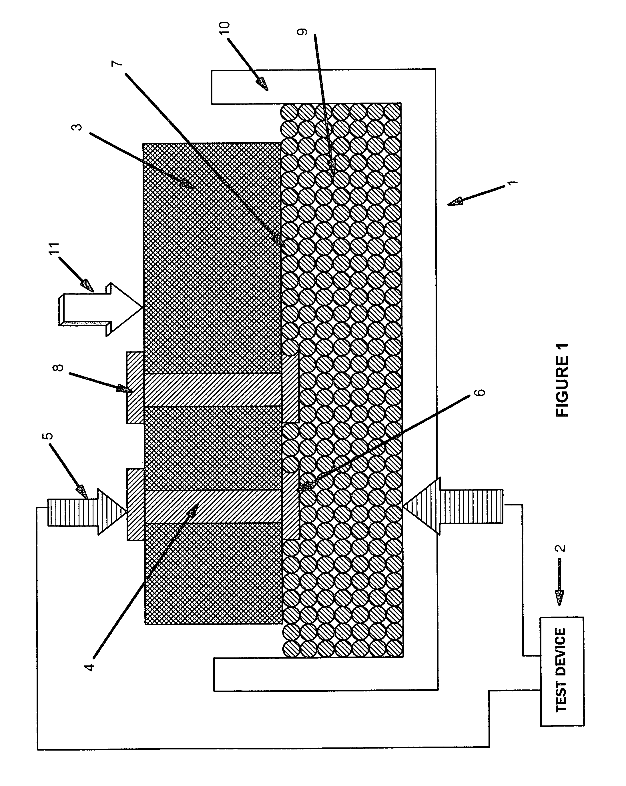
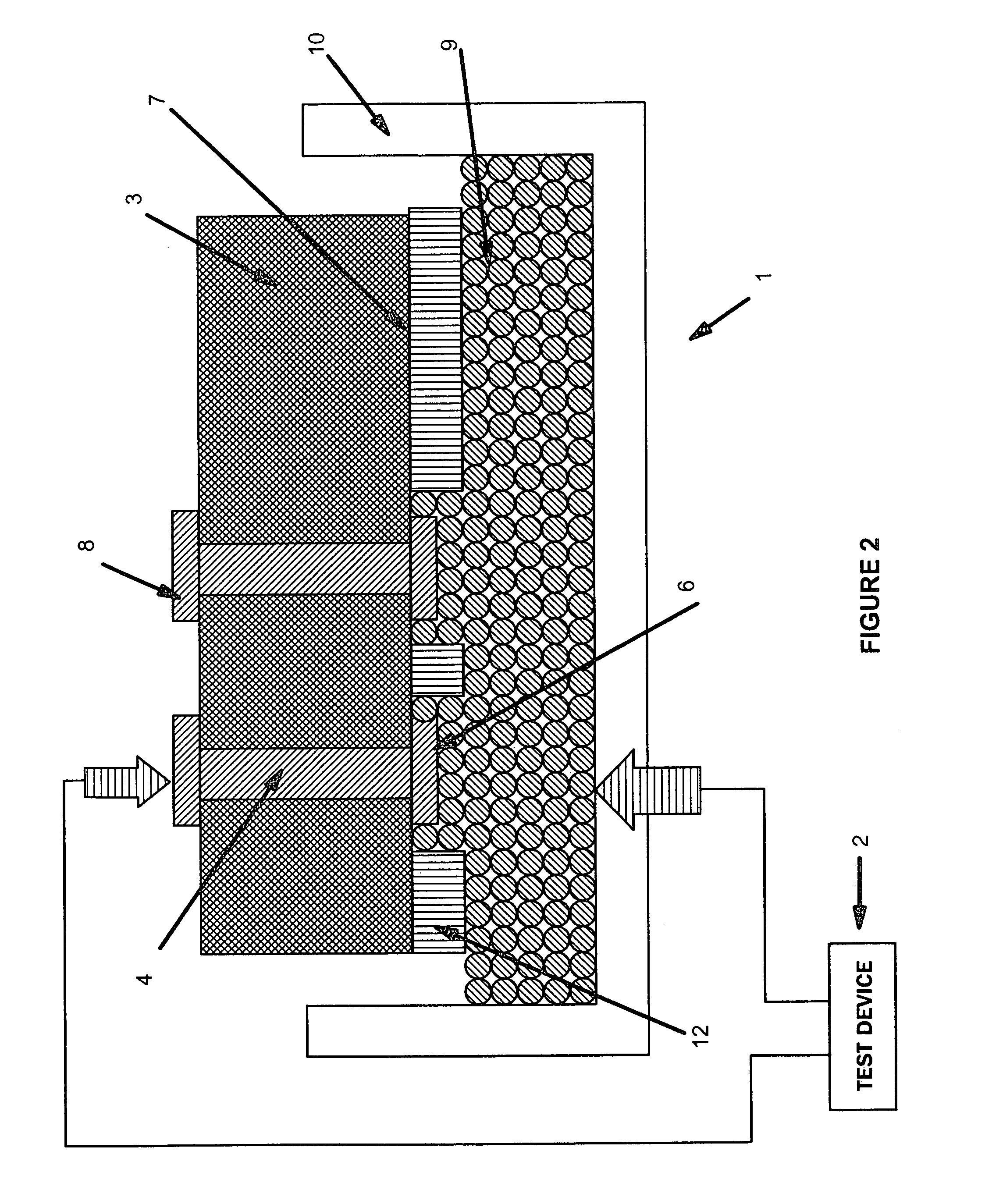
[0028]The term “electrically commoning” of contact pads or electronic circuits as used in this disclosure has the same meaning as electrically shorting of pads or circuits, as is well known in the art.

[0029]An overview of aspects and advantages of the subject invention to effect the described electrical commoning of circuitry and to carry out electrical testing of circuitry while eliminating known problems of the prior art, will first be described followed by a more detailed description with reference to the drawings.

[0030]The disclosed invention incorporates the use of small electrically conductive particles, preferably but not limited to spheres, placed in a receptacle so as to somewhat limit the horizontal spreading of the particles. A suitable quantity of the particles for the container or receptacle can be determined to ensure that the surface of a substrate containing a group of electrical contacts or pads to be shorted will always come into contact with a minimum concentratio...


PUM


Abstract

Improved methods and apparatus is disclosed for electrical testing of electronic circuits such as those existing in microcircuit devices including chip carriers, printed circuit boards and substrates. The invention provides for the testing of the continuity of electronic circuits in progressively smaller devices having increased density of circuits and having pads closely spaced. A quasi-fluidized bed of conductive particles is provided for effectively contacting pads on a first side of a substrate. Pads on another side of the substrate which are connected to the pads on the first side are then contacted by a test device. The circuit interconnecting respective pads on the two sides of the substrate can then be assessed for electrical continuity.

Description

BACKGROUND OF INVENTION[0001]This invention relates to electrical testing of electronic circuits and in particular improved methods and apparatus for testing electronic circuits such as those existing in chip carriers, printed circuit boards, substrates and other microcircuit devices.[0002]Flaws resulting in manufacturing processes of microcircuit devices can create undesired electrical conditions in electrical circuits contained within such devices resulting in flawed or inoperable electrical circuits wherein the flawed circuits do not function as originally intended and designed. In order to verify the electrical integrity of electronic circuits such as those present in chip carriers, printed circuit boards, electronic substrates or other microcircuit devices, during manufacture of such devices such circuits are typically submitted to electrical testing in an effort to detect unintended design flaws such as conditions of electrical shorts or opens in the circuits.[0003]There is a ...

Claims


Application Information

Patent Timeline
Patent Type & Authority Patents(United States)
IPC IPC(8): G01R31/08G01R31/02G01R1/04G01R1/067G01R31/28
CPCG01R31/2805G01R1/06711
Inventor DANOVITCH, DAVIDLANGLOIS, RICHARDLAPOINTE, MARTINLECLERC, ROBERT-PAUL
Owner TWITTER INC
Why Eureka
Try Eureka