Liquid crystal electro-optical device

a liquid crystal electrooptical and electrooptical technology, applied in optics, non-linear optics, instruments, etc., can solve the problems of liquid crystal alignment in the dark display state, decoloration phenomenon, and inability to accurately detect the color of the liquid crystal, etc., to achieve superiority in the effective utilization of light and high visual angle properties

Inactive Publication Date: 2006-05-02
SEMICON ENERGY LAB CO LTD
View PDF67 Cites 35 Cited by
  • Summary
  • Abstract
  • Description
  • Claims
  • Application Information

AI Technical Summary

Benefits of technology

[0037]The present invention provides a liquid crystal electro-optical device in which the disadvantages of conventional liquid crystal electro-optical devices are solved, and characterized by both the superiority in high visual angle properties characteristic of a liquid crystal electro-optical device operating in IPS mode and the superiority in effective utilization of light characteristic of a dispersion type liquid crystal electro-optical device.
[0045]The ratio of light scattered under no applied electric field can be increased by using a uniaxial polymer.
[0047]Thus, the ratio of the transmission of incident light under applied electric field to the scattering of incident light under no applied electric field can be increased to thereby realize a display having a high contrast ratio.
[0048]By employing the constitution above, a liquid crystal electro-optical device having an improved visual angle based on the birefringence effect and an improved contrast attributed to the increase in scattering effect under no applied electric field can be implemented, while also acquiring a bright display characteristic of a dispersion type liquid crystal electro-optical device which requires no polarizer sheets.
[0050]In the present invention, particularly selected are nematic liquid crystals having a positive or a negative dielectric anisotropy. The visual angle can be further increased by using a liquid crystal having small anisotropy in refractive index.

Problems solved by technology

However, in case of a liquid crystal electro-optical device based on the operation principle above, although a normal display state is realized when the display plane is viewed from the direction perpendicular thereto, the display becomes dark and unclear when the display plane is viewed from a direction oblique thereto; in case of a color display, moreover, a decoloring phenomenon occurs.
Furthermore, there is another problem in case of a liquid crystal electro-optical device above.
However, a first disadvantage of this constitution (operation in IPS mode) is the liquid crystal alignment in the dark display state, i.e., the OFF state of electric field.
In practice, however, alignment defects form depending on the state of rubbing, and a uniform alignment over the entire substrate cannot be obtained.
Accordingly, a uniform black display cannot be obtained in the practical display of black color.
This is a problem which cannot be neglected in making substrates large-sized.
A second disadvantage of the operation in IPS mode is that the intensity distribution of the electric field is non-uniform.
Accordingly, a uniformity on the entire display cannot be obtained due to the non-uniformity in the rise time.
A third disadvantage of the operation in IPS mode is the low opening ratio (low aperture ratio).
Thus, liquid crystal present on the upper side and in the vicinity thereof cannot be controlled.
Thus, there is a problem that a display with high contrast cannot be realized.
Another problem in the dispersion type liquid crystal electro-optical device is that, in the bright state, the liquid crystal molecules align themselves in such a manner that the major axes thereof become perpendicular to the substrate plane.
Similarly, in a dispersion type liquid crystal electro-optical device again, the problem of visual angle as described above also remains.
However, it has disadvantages in that it has difficulty in increasing the opening ratio (aperture ratio), that the electric field is non-uniform, and that the display plane becomes dark by the use of a polarizer sheet, etc.
However, on the other hand, as described above, it has difficulty in realizing an image with high contrast, and, similar to conventional liquid crystal electro-optical devices, it has a disadvantage in that it greatly depends on the visual angle.

Method used


Image

  • Liquid crystal electro-optical device
  • Liquid crystal electro-optical device
  • Liquid crystal electro-optical device

Examples


example 1

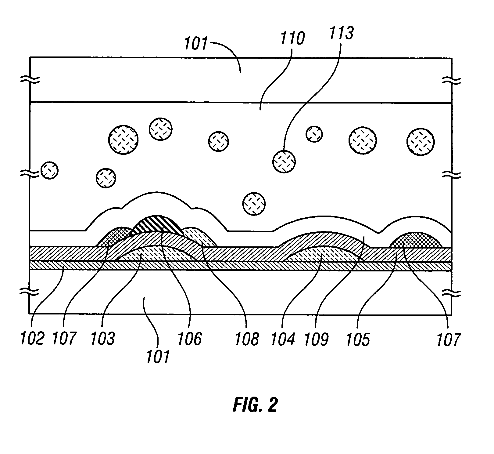
[0131]The present example describes the details of a process for fabricating a constitution according to the present invention with reference to FIGS. 1 and 2. More specifically, a case using a reverse stagger type thin film transistor as TFT is described.

[0132]Firstly, a silicon oxide film from 1,000 to 3,000 Å in thickness was formed as a base oxide film 102 on a Corning #7059 glass substrate 101 provided as an insulating substrate. The silicon oxide film can be formed, for example, by sputtering or by plasma CVD under an oxygen atmosphere.

[0133]Then, a Cr film for constituting a gate electrode 103 was formed at a thickness of from 1,000 to 5,000 Å. By patterning the Cr film, a pattern as a base for the gate electrode 103 can be formed.

[0134]Then, an isotropic plasma etching was performed thereafter by using a resist as a mask. Progressive etching was controlled and an electrode with a curved plane was formed by appropriately setting the discharge gas voltage. A gate electrode 103...

example 2

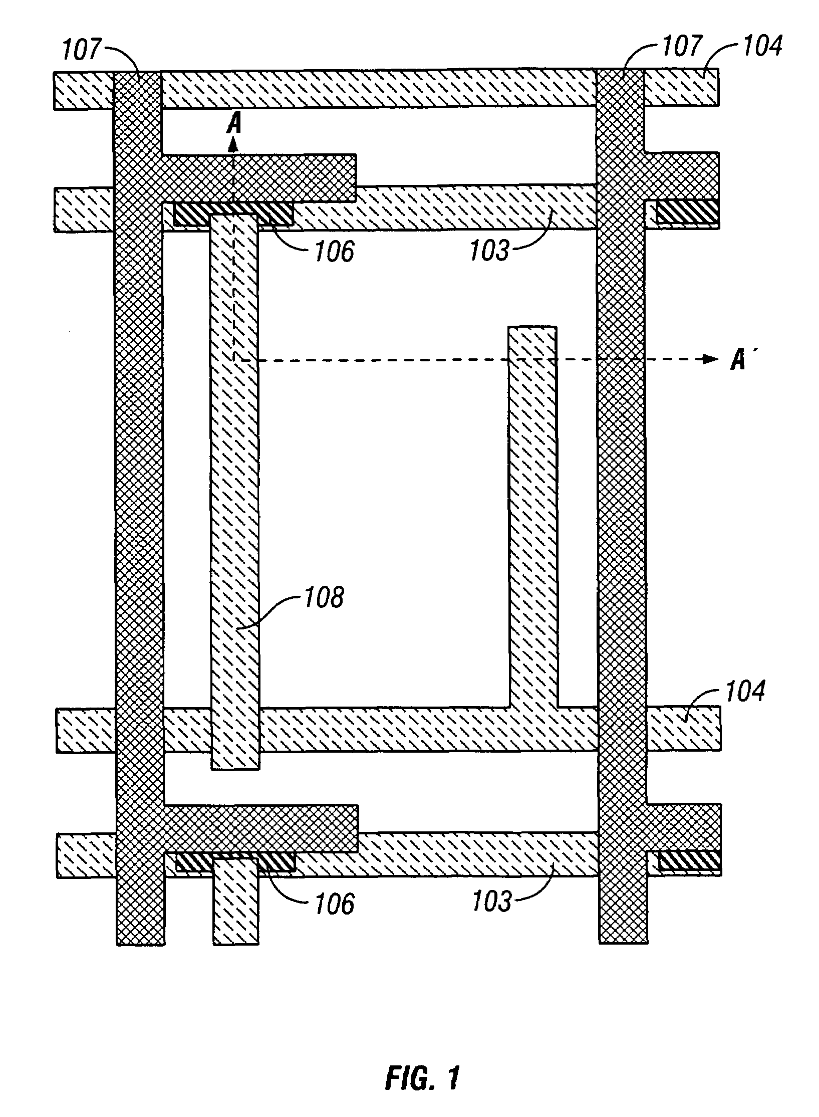
[0147]The present Example refers to a monolithic active matrix circuit whose peripheral drive circuit is also formed on the substrate. The process for fabricating the liquid crystal electro-optical device according to the present Example is explained below by making reference to FIGS. 3 and FIGS. 4(A) to 4(F).

[0148]Referring to FIG. 3 showing a scheme of the periphery of a pixel portion of the present Example. FIGS. 4(A) to 4(F) show the cross section taken along line B–B′–B″ in FIG. 3. In FIGS. 4(A) to 4(F), the left hand side shows the process steps for fabricating the TFT of a drive circuit, whereas the right side shows the process steps for fabricating the TFT of an active matrix circuit.

[0149]Firstly, a silicon oxide film was formed as a base film on a glass substrate 301. In the present case, a silicon oxide film was formed on a Corning #1737 glass substrate by sputtering method.

[0150]An amorphous silicon film was formed thereafter by plasma CVD or by LPCVD to a thickness of f...

example 3

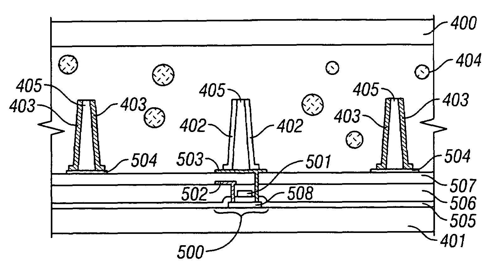
[0176]The present Example explains in detail the constitution of a liquid crystal electro-optical device with reference to FIGS. 7(A) and 7(B). An active matrix circuit consisting of a thin film transistor 500 and a common electrode 403 is formed on a substrate 401. The constitution of the active matrix circuit is shown in FIG. 10.

[0177]In FIGS. 7(A) and 7(B), single pixel is defined by the effective area of an electric field formed between the electrodes 402 provided on both side planes of a support 405 constituting a wall, and the electrodes 403 provided on two supports 405.

[0178]The drain electrodes 402 were formed on both side planes of the wall 405 made from an insulating material. The drain electrode was insulated per pixel. Furthermore, a polyimide resin was used as the insulating material constituting the wall.

[0179]Referring to FIG. 7(A), an island-like silicon film 508 is provided on a glass substrate 401 having thereon an undercoat film (not shown in the figure), and an a...


PUM

PropertyMeasurementUnit
angleaaaaaaaaaa
widthaaaaaaaaaa
widthaaaaaaaaaa

Abstract

A brighter active matrix type liquid crystal electro-optical device with a higher contrast, yet having a wider visual angle is realized, said liquid crystal electro-optical device comprises a liquid crystal layer and means for applying an electric field to the liquid crystal layer in the direction parallel to the substrate, wherein the liquid crystal layer comprises a liquid crystal material dispersed in a polymer material. Also a liquid crystal electro-optical device comprising a liquid crystal layer disposed on a substrate is included, wherein the transmission mode or the dispersion mode of an incident light is selected by an electric field applied to the liquid crystal layer in the direction parallel to the liquid crystal layer.

Description

CROSS-REFERENCE TO RELATED APPLICATIONS[0001]This application is a divisional application of U.S. application Ser. No. 10 / 202,221, filed on Jul. 23, 2002, now allowed, which is a continuation of U.S. application Ser. No. 08 / 789,458, filed on Jan. 27, 1997, now U.S. Pat. No 6,449,024 which claims the benefit of foreign priority applications filed in Japan on Jan. 26, 1996, as Application No. 8-032926 and on Jan. 29, 1997, as Application No. 8-035457. This application claims priority to all of these applications, and all of these applications are incorporated by reference.BACKGROUND OF THE INVENTION[0002]The present invention relates to a liquid crystal electro-optical device having excellent electric properties and contrast, and which is capable of realizing a bright and uniform display over the entire image plane.[0003]According to the basic principle for the operation and the display of a liquid crystal electro-optical device, in general, a liquid crystal electro-optical device has...

Claims


Application Information

Patent Timeline
Patent Type & Authority Patents(United States)
IPC IPC(8): G02F1/1343G02F1/1334
CPCG02F1/1334G02F1/134363G02F1/134336
Inventor HIRAKATA, YOSHIHARUNISHI, TAKESHISATAKE, RUMO
Owner SEMICON ENERGY LAB CO LTD
Why Eureka
Try Eureka