Double data rate synchronous dynamic random access memory semiconductor device

a semiconductor device and synchronous dynamic random access technology, applied in the field of semiconductor memory devices, can solve problems such as the malfunction of ddr sdram semiconductor devices

Inactive Publication Date: 2006-05-02
SAMSUNG ELECTRONICS CO LTD
View PDF5 Cites 18 Cited by
  • Summary
  • Abstract
  • Description
  • Claims
  • Application Information

AI Technical Summary

Benefits of technology

[0011]These and other drawbacks and disadvantages of the prior art are addressed by a semiconductor memory device that prevents a conflict between data read from the device and data written to the device.

Problems solved by technology

However, since the clock signal CLK_DLL has not been input to the output controller, the output controller may erroneously apply an active read command RD latched therein to the output buffer to activate the output buffer.
Such a conflict causes malfunction of the DDR SDRAM semiconductor device.

Method used


Image

  • Double data rate synchronous dynamic random access memory semiconductor device
  • Double data rate synchronous dynamic random access memory semiconductor device
  • Double data rate synchronous dynamic random access memory semiconductor device

Examples


Embodiment Construction

[0019]The present invention will now be described more fully with reference to the accompanying drawings, in which preferred embodiments of the invention are shown. In the drawings, the same reference numerals have been used, where possible, to designate the same elements.

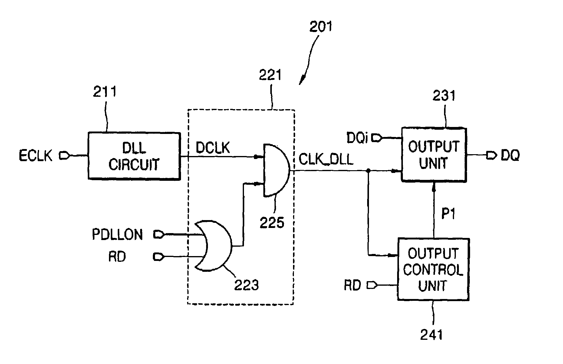
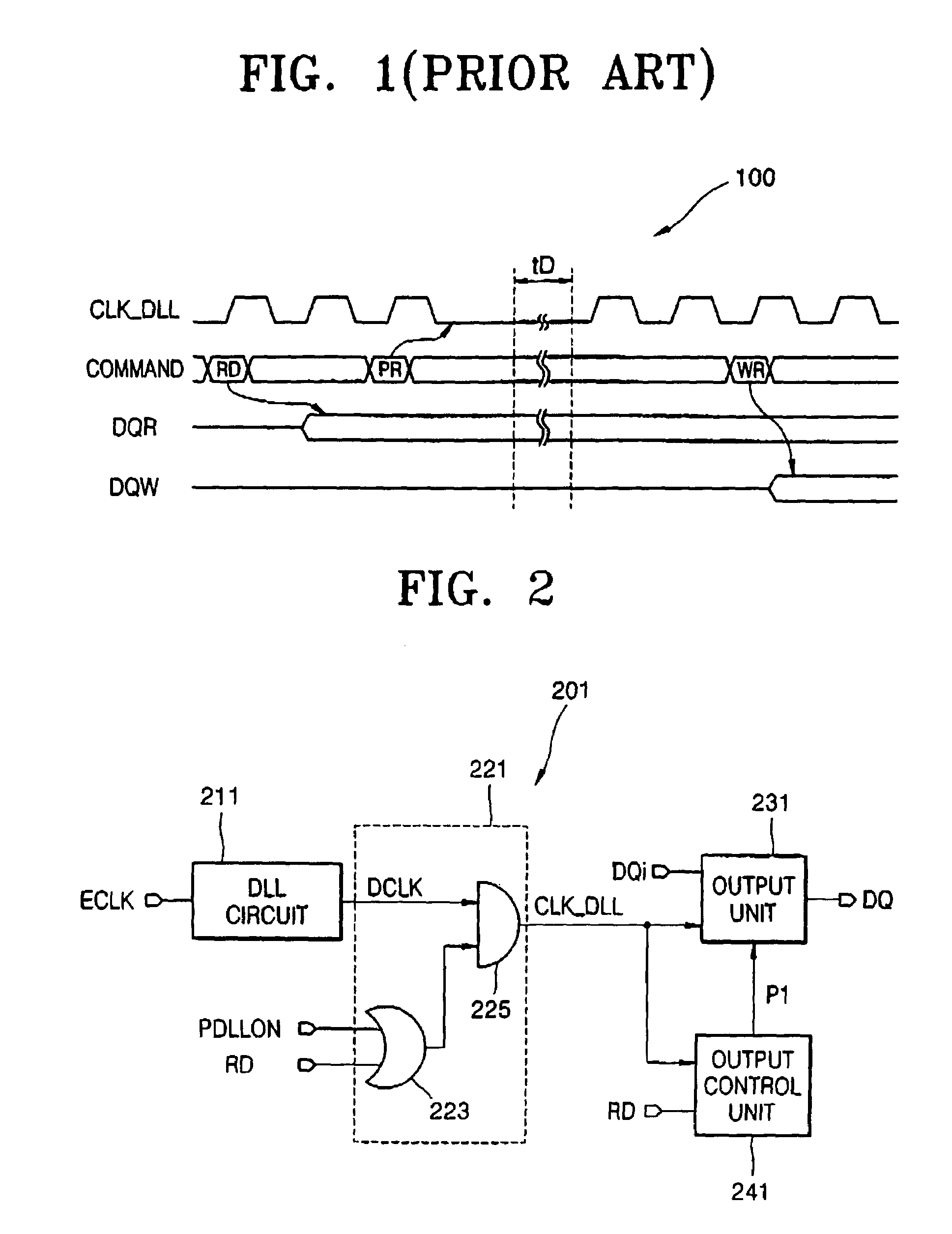
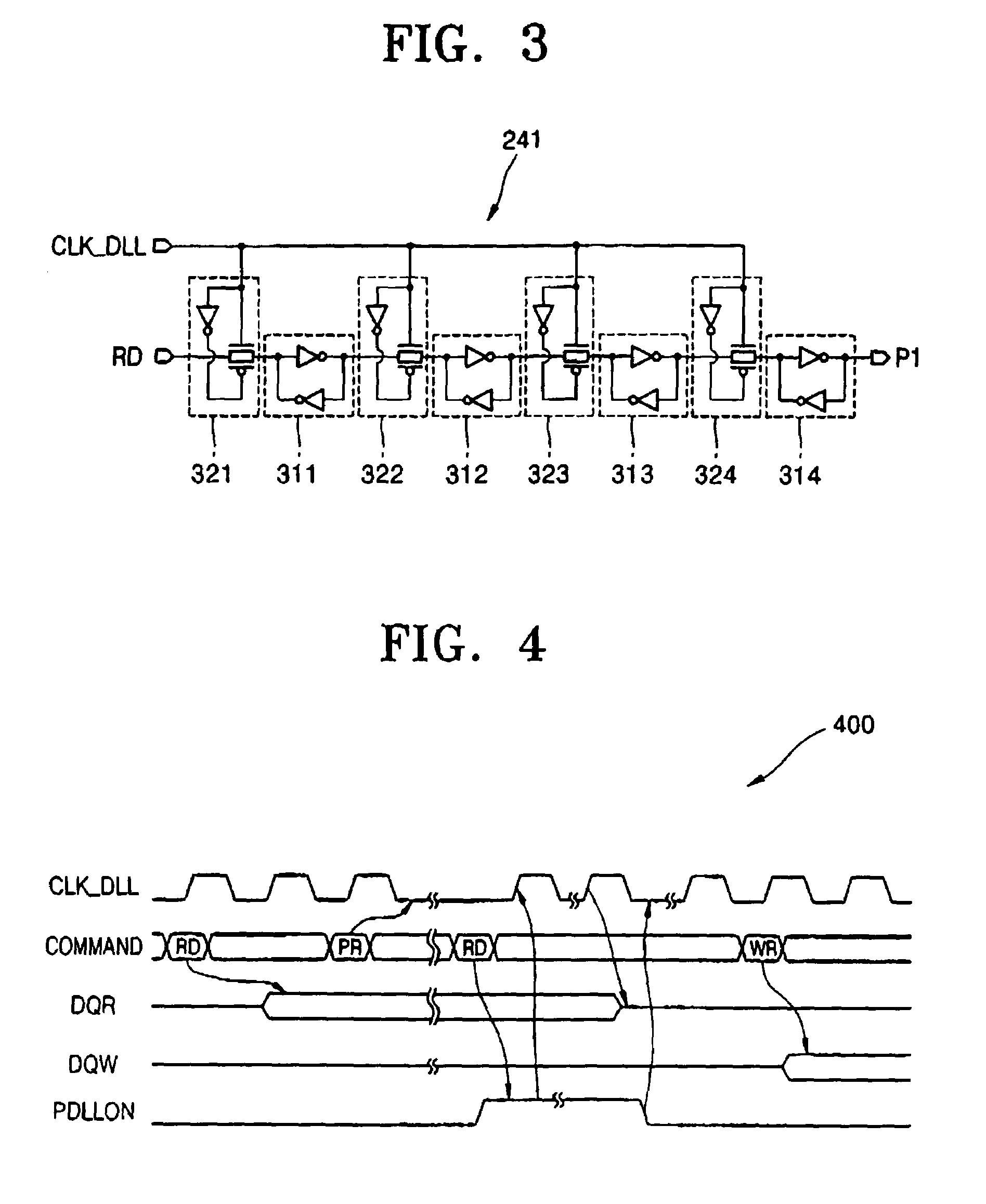
[0020]FIG. 2 shows a block diagram illustrating a double data rate (“DDR”) synchronous dynamic random access memory (“SDRAM”) semiconductor device according to the present invention. Referring to FIG. 2, a DDR SDRAM semiconductor device 201 includes a delay locked loop (“DLL”) circuit 211, a clock signal control unit 221, an output control unit 241, and an output unit 231.

[0021]The DLL circuit 211 compensates for skew of an input clock signal ECLK and generates an output clock signal DCLK. The clock signal control unit 221 includes a first logic unit 223 and a second logic unit 225.

[0022]The first logic unit 223 receives a read signal RD and a DLL locking signal PDLLON. When either the read signal RD or the DLL loc...


PUM


Abstract

A double data rate (“DDR”) synchronous dynamic random access memory (“SDRAM”) semiconductor device is provided that prevents a conflict between data read from and data written to the DDR SDRAM semiconductor device when data is written to the DDR SDRAM semiconductor device, which includes a delay locked loop (“DLL”) circuit, a clock signal control unit, an output unit, and an output control unit, where the DLL circuit compensates for skew of an input clock signal and generates an output clock signal; the clock signal control unit receives a read signal activated when data stored in the DDR SDRAM semiconductor device is read out, a DLL locking signal activated when the DLL circuit performs a locking operation on the input clock signal, and the output clock signal, and outputs the output clock signal when either the read signal or the DLL locking signal is active; the output unit buffers data stored in the DDR SDRAM semiconductor device and outputs the data to outside of the DDR SDRAM semiconductor device in synchronization with the output clock signal output from the clock signal control unit; and the output control unit receives the output clock signal output from the clock signal control unit, and the read signal, and outputs the read signal to the output unit in synchronization with the output clock signal output from the clock signal control unit.

Description

CROSS REFERENCE TO RELATED APPLICATION[0001]This application claims foreign priority under 35 U.S.C. § 119 to Korean Patent Application No. 2003-13423, filed on 4 Mar. 2003, in the Korean Intellectual Property Office.BACKGROUND OF THE INVENTION[0002]1. Field of the Invention[0003]The present invention relates to semiconductor memory devices, and more particularly, to semiconductor memory devices that prevent conflicts between data read from and data written to the devices.[0004]2. Description of the Related Art[0005]In general, a DDR SDRAM semiconductor device is connected to a DRAM controller. The DRAM controller writes data to and reads data from the DDR SDRAM semiconductor device. The DDR SDRAM semiconductor device includes a memory bank that stores data, a delay locked loop (“DLL”) circuit that generates a clock signal, an output buffer that buffers data stored in the memory bank and outputs the buffered data in synchronization with the clock signal, and an output controller tha...

Claims


Application Information

Patent Timeline
Patent Type & Authority Patents(United States)
IPC IPC(8): G11C7/00G11C11/40G11C7/10G11C7/22G11C8/00G11C11/407
CPCG11C7/1051G11C7/1066G11C7/222G11C7/1078G11C7/1093G11C7/1072G11C11/40
Inventor SEO, SUNG-MINKIM, CHI-WOOKKIM, KYU-HYOUN
Owner SAMSUNG ELECTRONICS CO LTD
Why Eureka
Try Eureka