Sidewall magnet improving uniformity of inductively coupled plasma and shields used therewith

a technology of inductively coupled plasma and shields, applied in the field of materials sputtering, can solve the problems of poor sidewall coverage, thin sidewall portions, and the etching performed by such an apparatus is found to be very non-uniform across the diameter of the wafer, and achieve the effect of improving the radial uniformity of sputter etching of the substra

Inactive Publication Date: 2006-05-09
APPLIED MATERIALS INC
View PDF33 Cites 30 Cited by
  • Summary
  • Abstract
  • Description
  • Claims
  • Application Information

AI Technical Summary

Benefits of technology

[0013]One aspect of the invention related to plasma sputtering includes a magnetic ring positioned in back of a coil and having a magnetic polarity along the axis of the coil. The coil may be used both for inducing a plasma near the substrate being processed, particularly for sputter etching the substrate, and as a secondary target for sputter deposition. Changing between or combining the two processes depends upon RF and DC biasing conditions on the coil as well as on the target and wafer biasing. The magnetic ring produces an axial DC magnetic field adjacent the coil that acts as a plasma barrier and thereby prevents the plasma inductively created by the coil from being grounded to the coil before it diffuses or is otherwise attracted to the substrate, thereby improving the radial uniformity of sputter etching of the substrate. The axial DC magnetic field also acts as a magnetron for sputtering of the coil.

Problems solved by technology

Sidewall coverage is generally poor and produces thin sidewall portions 22 deep inside the bole 16.
However, the etching performed by such an apparatus has been found to be very non-uniform across the diameter of the wafer.
A further problem, particularly with the recently developed 300 mm chambers, is that the size of the chamber needs to be minimized to reduce the foot print of the reactor in valuable clean room space.

Method used


Image

  • Sidewall magnet improving uniformity of inductively coupled plasma and shields used therewith
  • Sidewall magnet improving uniformity of inductively coupled plasma and shields used therewith
  • Sidewall magnet improving uniformity of inductively coupled plasma and shields used therewith

Examples


Embodiment Construction

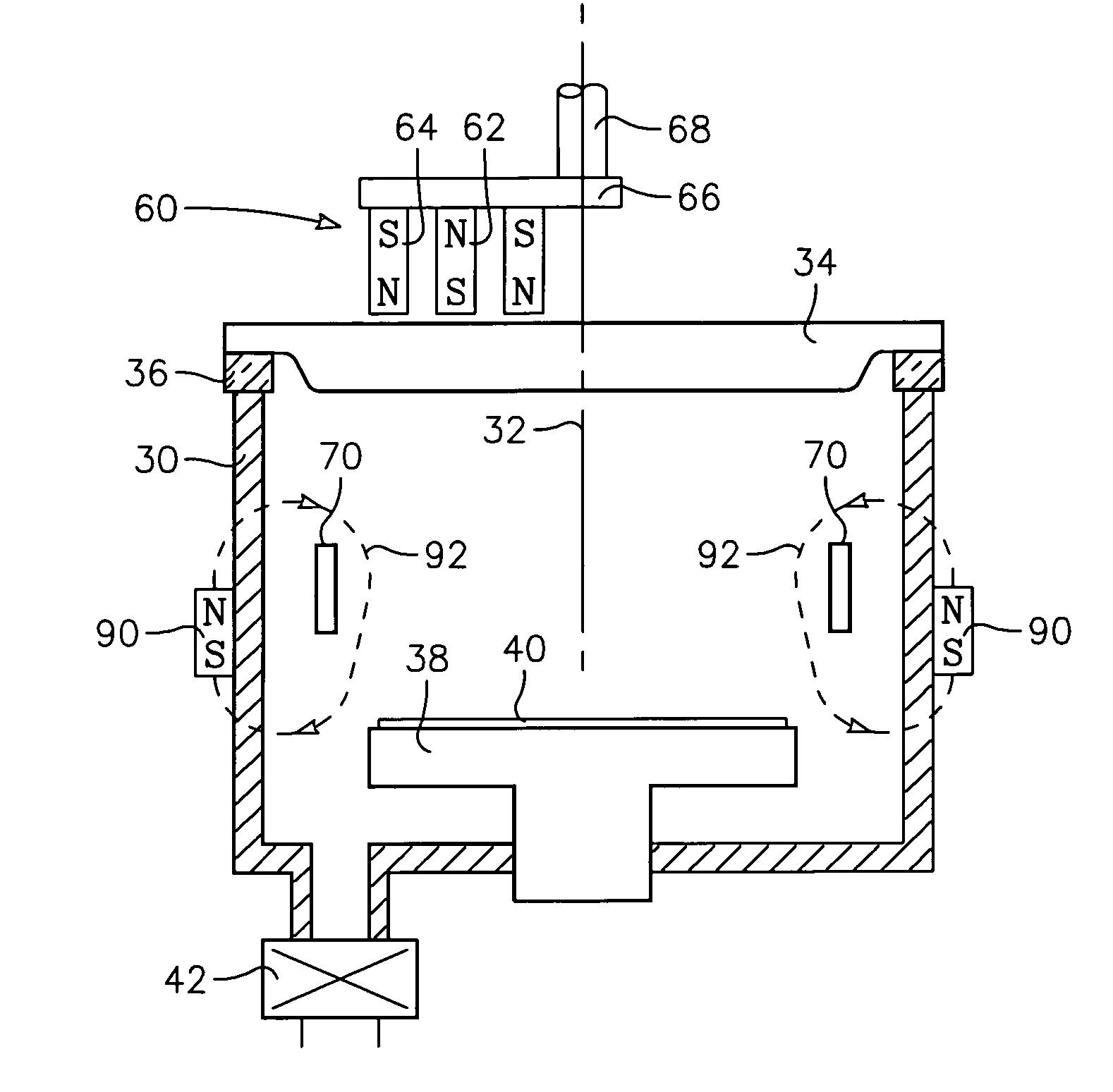
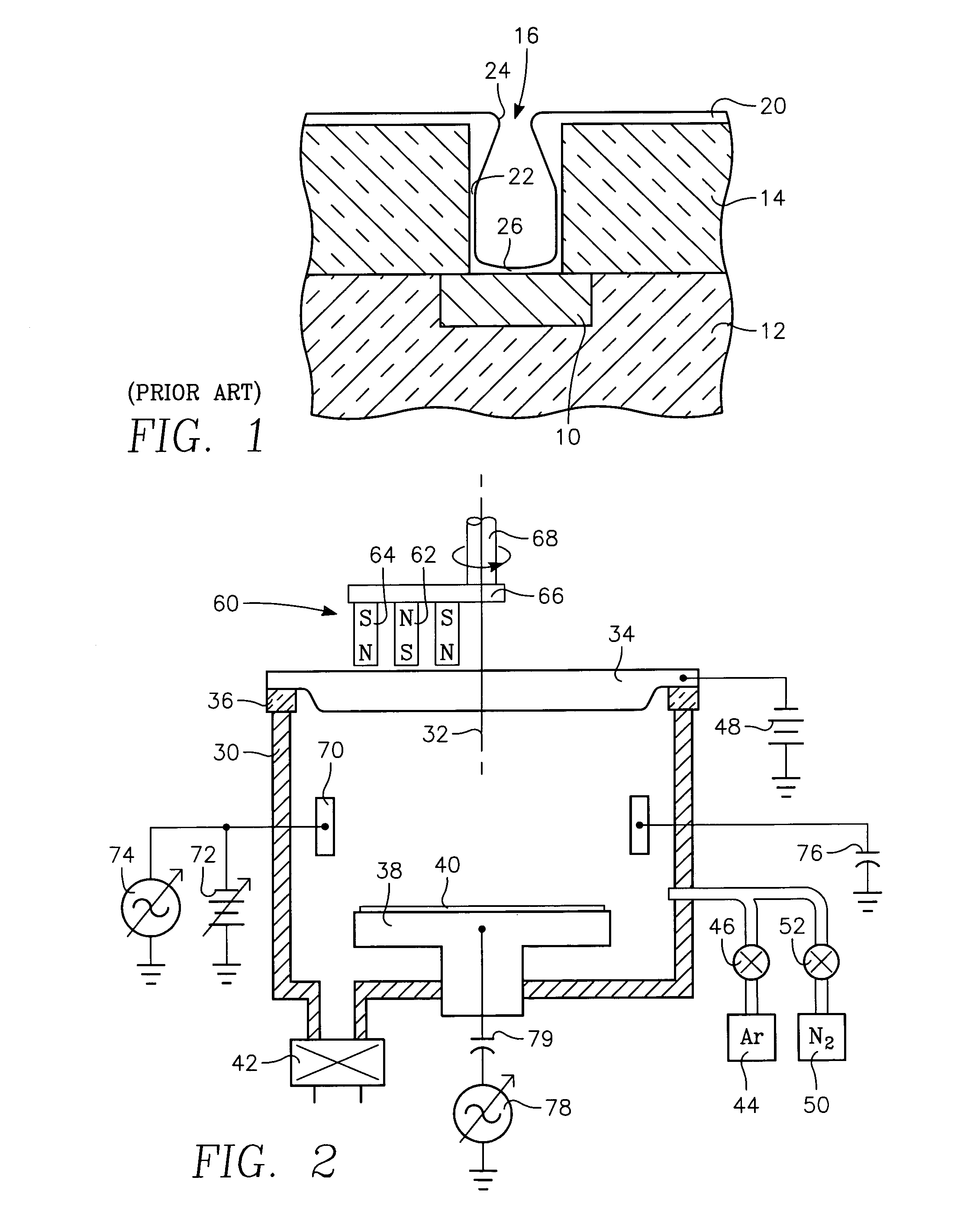
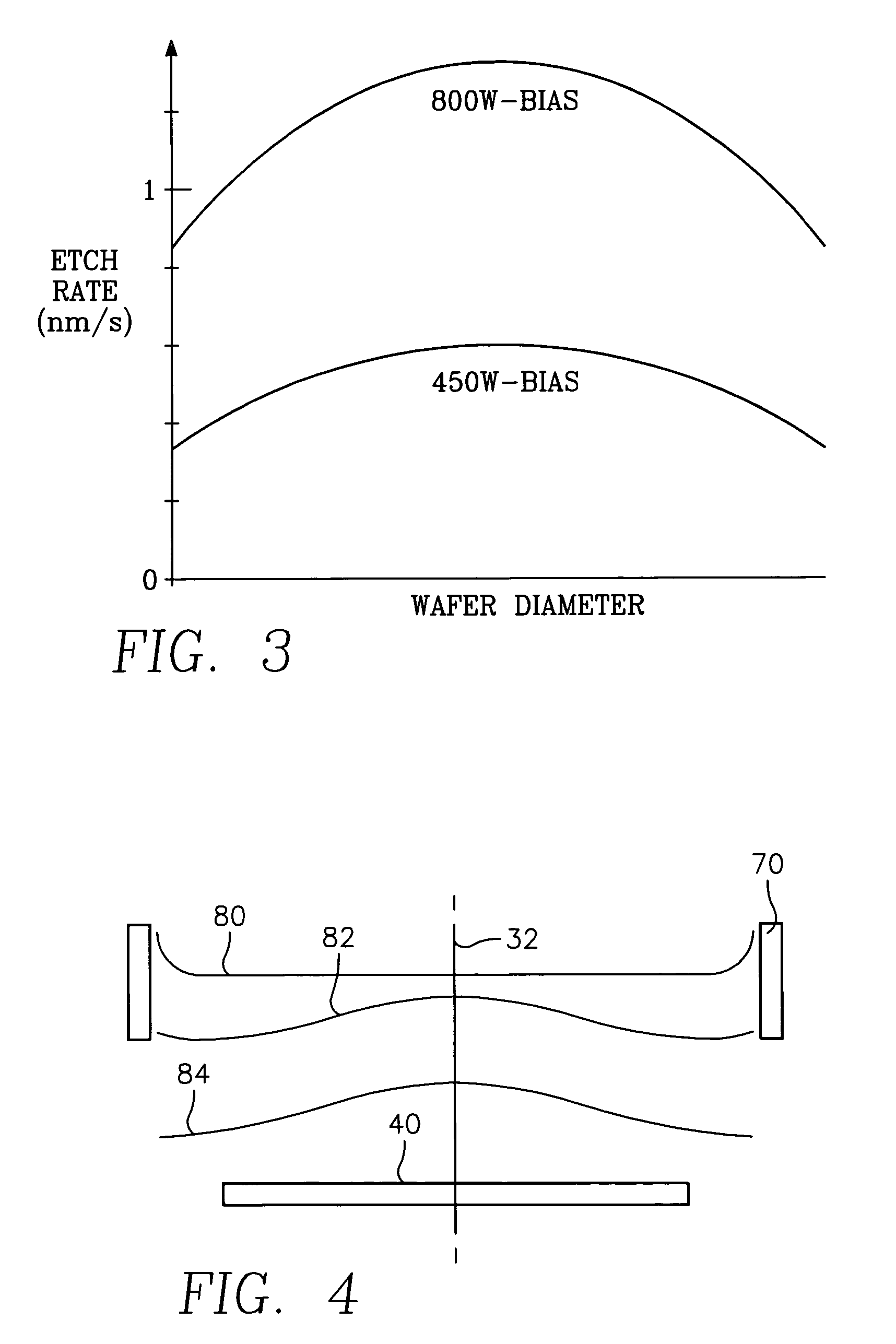
[0030]A mechanism believed to be responsible for the non-uniform rate will be explained with reference tote schematic illustration of FIG. 4. The RF inductive coil 70 creates an initial plasma distribution 80 that is largely concentrated near the coil 70. The edge localization is explainable in terms of the skin depth of the plasma being created. The RF coil 70 produces an RF magnetic field generally along the central axis 32. The RF magnetic field in turn generates an azimuthal electric field which excites an azimuthal current which in turn supports the plasma and increases its density. However, the electric field in turn is electrically shorted by the highly conductive plasma. That is, the RF field reaches into the plasma only to the skin depth of the plasma. However, the plasma diffuses, as shown by distribution 82, in the axial direction towards the wafer 40 and also radially. The radial diffusion includes inward components towards the central axis 32 and outward components towa...


PUM

PropertyMeasurementUnit
aspect ratioaaaaaaaaaa
pressureaaaaaaaaaa

Abstract

One aspect of the invention includes an auxiliary magnet ring positioned outside of the chamber wall of a plasma sputter reactor and being disposed at least partially radially outwardly of an RF coil used to inductively generate a plasma, particularly for sputter etching the substrate being sputter deposited. Thereby, a magnetic barrier prevents the plasma from leaking outwardly to the coil and improves the uniformity of sputter etching. The magnetic field also acts as a magnetron when the coil, when made of the same material as the primary target, is being used as a secondary target. Another aspect of the invention includes a one-piece inner shield extending from the target to the pedestal with a smooth inner surface and supported by an annular flange in a middle portion of the shield. The shield may be used to support the RF coil.

Description

RELATED APPLICATIONS[0001]This application is a continuation in part of International Application PCT / US02 / 36940, filed Nov. 14, 2002, which is a continuation in part of Ser. No. 09 / 993,543, filed Nov. 14, 2001, now issued as U.S. Pat. No. 6,610,184, both of which are incorporated by reference herein in their entireties.FIELD OF THE INVENTION[0002]The invention relates generally to sputtering of materials. In particular, the invention relates to the auxiliary magnets used in an inductively coupled plasma reactor. It also relates to shields used in a sputter reactor.BACKGROUND ART[0003]Sputtering, alternatively called physical vapor deposition (PVD), is the most prevalent method of depositing layers of metals and related materials in the fabrication of semiconductor integrated circuits. One application of sputtering is to deposit barrier and seed layers associated with a via structure illustrated in cross-section in FIG. 1. A conductive feature 10 is formed in the surface of a lower ...

Claims


Application Information

Patent Timeline
Patent Type & Authority Patents(United States)
IPC IPC(8): C23C14/35C23C14/04H05H1/46C23C14/34H01J37/32H01J37/34H01L21/285H01L21/768
CPCC23C14/046H01L21/76877C23C14/3457C23C14/358H01J37/321H01J37/32623H01J37/3402H01J37/3408H01J37/3411H01J37/3441H01L21/2855H01L21/76838H01L21/76843C23C14/345H01J2237/3327H01J37/34H01J37/32
Inventor GUNG, TZA-JINGTANG, XIANMINFORSTER, JOHNDING, PEIJUNSCHWEITZER, MARCMILLER, KEITH A.LAVITSKY, ILYA
Owner APPLIED MATERIALS INC
Why Eureka
Try Eureka