Sputtering Target for PVD Chamber

a sputtering target and chamber technology, applied in the field of physical vapor deposition, can solve the problem of preventing film thickness uniformity from being achieved, and achieve the effect of improving the radial uniformity of the sputtering process

Active Publication Date: 2017-12-07
APPLIED MATERIALS INC
View PDF0 Cites 0 Cited by
  • Summary
  • Abstract
  • Description
  • Claims
  • Application Information

AI Technical Summary

Benefits of technology

[0015]Another aspect pertains to a method of improving radial uniformity of a sputtering process in a sputtering chamber comprising: disposing a target in the sputtering chamber in a spaced relationship with a substrate having a radial surface facing the target, the target comprising a front face defining sputterable target surface extending between peripheral edges of the target and the sputterable target surface defining an overall concave shape substantially between the peripheral edges; and sputtering material from the target such that material from the target is uniformly deposited across the radial surface of the substrate.

Problems solved by technology

In recent development of semiconductor industry, especially in high dielectric constant and metal gate applications, there is a stringent requirement of good uniformity for thin films on the order of 1 to 5 Angstroms, which poses a challenge to the traditional physical vapor deposition (PVD).
In magnetron sputtering with longer spacing from target surface to the wafer, the film at wafer central region tends to be much thicker than the other locations on the wafer, which prevents film thickness uniformity from being achieved.

Method used


Image

  • Sputtering Target for PVD Chamber
  • Sputtering Target for PVD Chamber
  • Sputtering Target for PVD Chamber

Examples


Embodiment Construction

[0038]Before describing several exemplary embodiments of the invention, it is to be understood that the invention is not limited to the details of construction or process steps set forth in the following description. The invention is capable of other embodiments and of being practiced or being carried out in various ways.

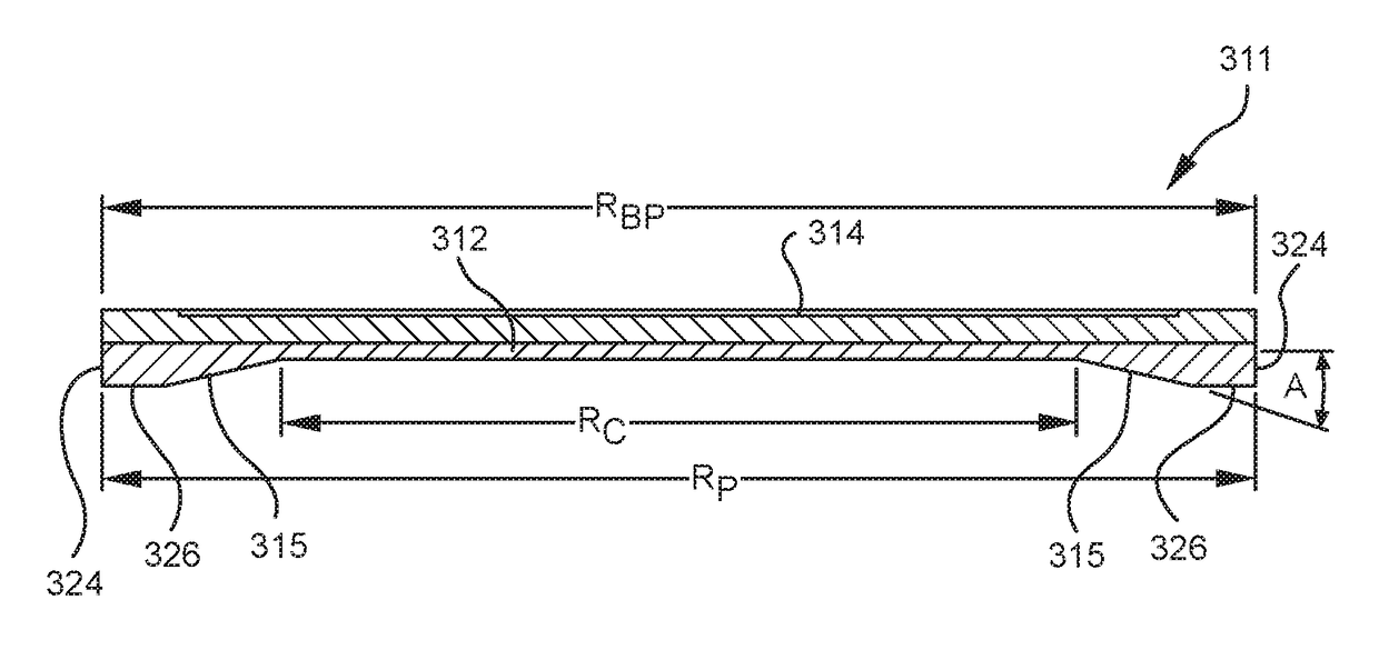
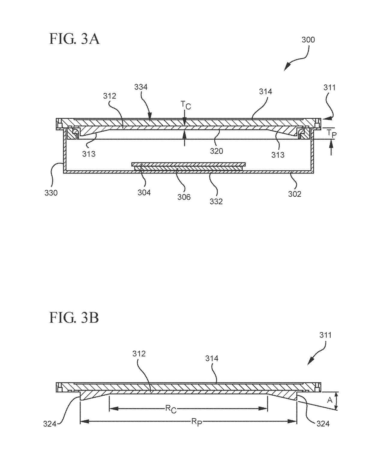
[0039]Referring now to FIGS. 3A and 3B a first embodiment of a process chamber with a target having a generally concave shape is shown. FIG. 3A shows a semiconductor fabrication chamber 300 according to a first embodiment, comprising a chamber body 302 and a substrate 304 supported by a substrate support 306 within the chamber body 302. The substrate support 306 may be electrically floating or may be biased by a pedestal power supply (not shown). A target assembly 311 includes a target 312 supported by a backing plate 314. The target 312 includes a front face including sputterable area 320 of disposed in a spaced relationship with respect to the substrate support 30...


PUM

PropertyMeasurementUnit
angleaaaaaaaaaa
angleaaaaaaaaaa
angleaaaaaaaaaa

Abstract

Target assemblies and PVD chambers including target assemblies are disclosed. The target assembly includes a target that has a concave shaped target. When used in a PVD chamber, the concave target provides more radially uniform deposition on a substrate disposed in the sputtering chamber.

Description

CROSS-REFERENCE TO RELATED APPLICATIONS[0001]This application is a Continuation of U.S. patent application No. Ser. 12 / 723,199, filed Mar. 12, 2010, now U.S. Pat. No. _____, issued _____, the entire disclosure of which is hereby incorporated by reference.FIELD OF THE INVENTION[0002]Embodiments of the present invention generally pertain to the field of physical vapor deposition. More specifically, embodiments of the invention relate to a concave sputtering target design to improve film uniformity of films deposited within a physical vapor deposition chamber, chambers including a concave sputtering target and methods of sputtering material onto a substrate using a concave target.BACKGROUND[0003]Sputtering is a physical vapor deposition (PVD) process in which high-energy ions impact and erode a solid target and deposit the target material on the surface of a substrate such as a semiconductor substrate, a specific example being a silicon wafer. In semiconductor fabrication, the sputteri...

Claims


Application Information

Patent Timeline
Patent Type & Authority Applications(United States)
IPC IPC(8): C23C14/34H01J37/34
CPCC23C14/3407H01J37/342H01J37/3423
Inventor LIU, ZHENDONGWANG, RONGJUNTANG, XIANMINGANDIKOTA, SRINIVASGUNG, TZA-JINGRASHEED, MUHAMMAD M.
Owner APPLIED MATERIALS INC
Why Eureka
Try Eureka