Methods for fabricating interposers including upwardly protruding dams

a technology of interposers and dams, which is applied in the field of interposers, can solve the problems of voids or bubbles, the introduction of underfill materials between a semiconductor die and an interposer secured thereto is somewhat undesirable, and the conventional semiconductor device package is relatively bulky, etc., to facilitate the formation of electrical connections, impart stability to the assembly, and low viscosity encapsulant material

Inactive Publication Date: 2006-05-09
MICRON TECH INC
View PDF78 Cites 10 Cited by
  • Summary
  • Abstract
  • Description
  • Claims
  • Application Information

AI Technical Summary

Benefits of technology

[0024]An interposer according to the present invention may include one or more slots or apertures formed completely therethrough. In one embodiment of the interposer, an elongate, substantially centrally located slot facilitates the formation of electrical connections from the bond pads of a semiconductor die with one or more substantially centrally located rows of bond pads to corresponding first contact pads located near the slot of the interposer. Electrical traces carried by the interposer connect each first contact pad to a corresponding second contact pad on an upper surface of the interposer opposite from the semiconductor die. The second contact pads are disposed in an array over the surface of the interposer. The upwardly protruding dam at least partially laterally surrounds the slot and at least the first contact pads of the interposer and, preferably, substantially completely laterally surrounds the slot and first contact pads.
[0025]The interposer may be assembled with a semiconductor die by placing one or more dielectric, adhesive strips between the active surface of the semiconductor die and a lower surface of the interposer. The dielectric, adhesive strips at least partially laterally surround the bond pads on the active surface of the semiconductor die, as well as impart st

Problems solved by technology

Due to the ever-decreasing sizes of state of the art electronic devices, conventional semiconductor device packages are relatively bulky.
The introduction of underfill materials between a semiconductor die and an interposer secured thereto is somewhat undesirable since an additional assembly step is required.
Moreover, as conventional underfill materials flow into the spaces between a semiconductor die and an interposer, voids or bubbles may form and remain therein.
In addition, the use of glob-top type encapsulants to protect the bond pads and intermediate conductive elements of such chip-scale packages is somewhat undesirable since glob-top encapsulants may flow laterally over the second contact pads or conductive structures protruding therefrom.
While more viscous encapsulant materials may be used, because viscous glob-top encapsulants typically cure with a convex surface, the amount of encapsulant needed to adequately protect the bond wires or other intermediate conductive elements between the bond pads and first contact pads may result in a glob-top that protrudes an undesirable distance from the interposer, which may require the removal of some of the convex portion of the glob-top or the use of undesirably long conductive elements between the second contact pads of the interposer and the contact pads of the carrier substrate.
As the lower, peripheral portion of the interposer must have a sufficient thickness and rigidity to support the first contact pads thereon and since the difference in height between the peripheral and centra

Method used


Image

  • Methods for fabricating interposers including upwardly protruding dams
  • Methods for fabricating interposers including upwardly protruding dams
  • Methods for fabricating interposers including upwardly protruding dams

Examples


Embodiment Construction

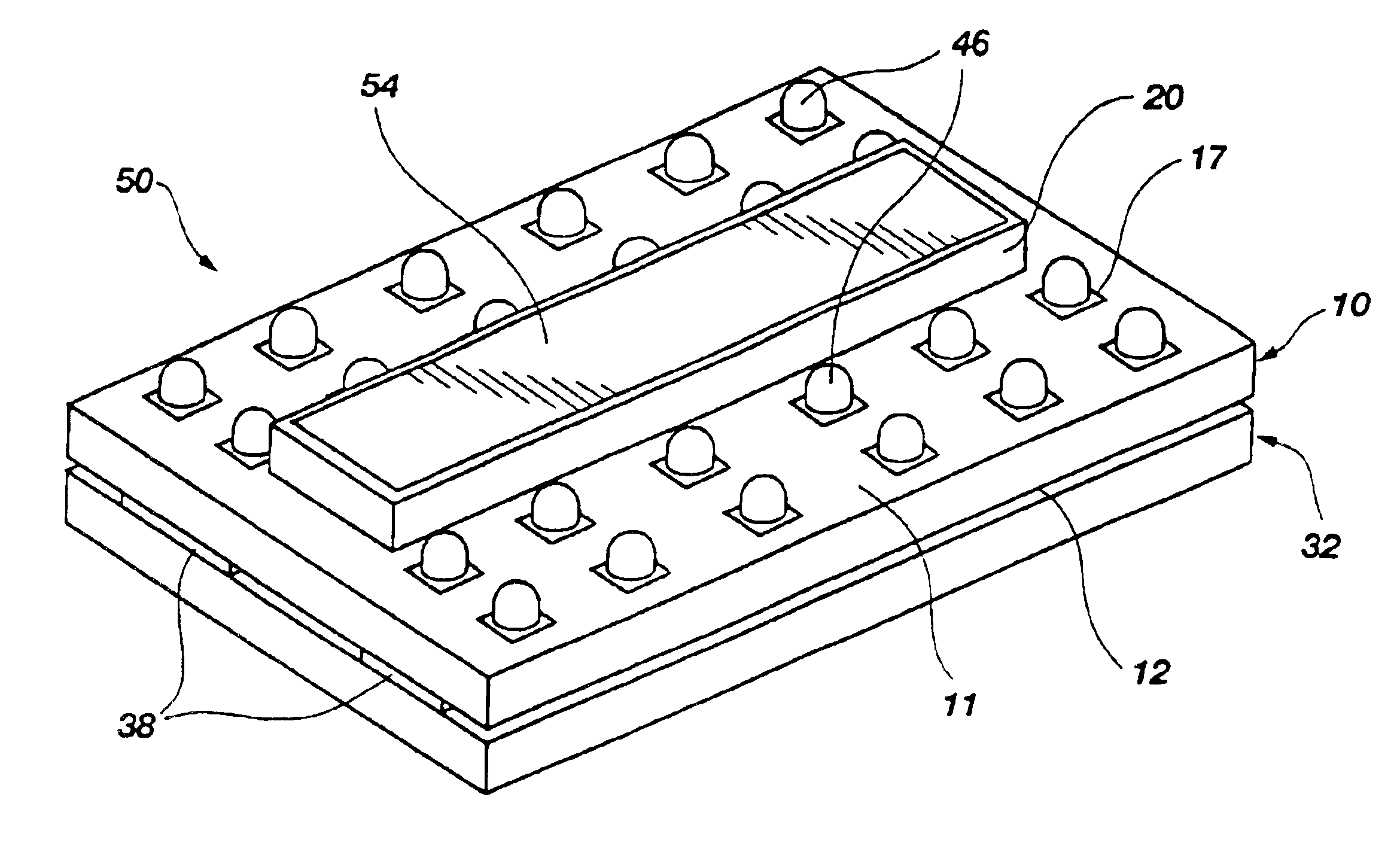
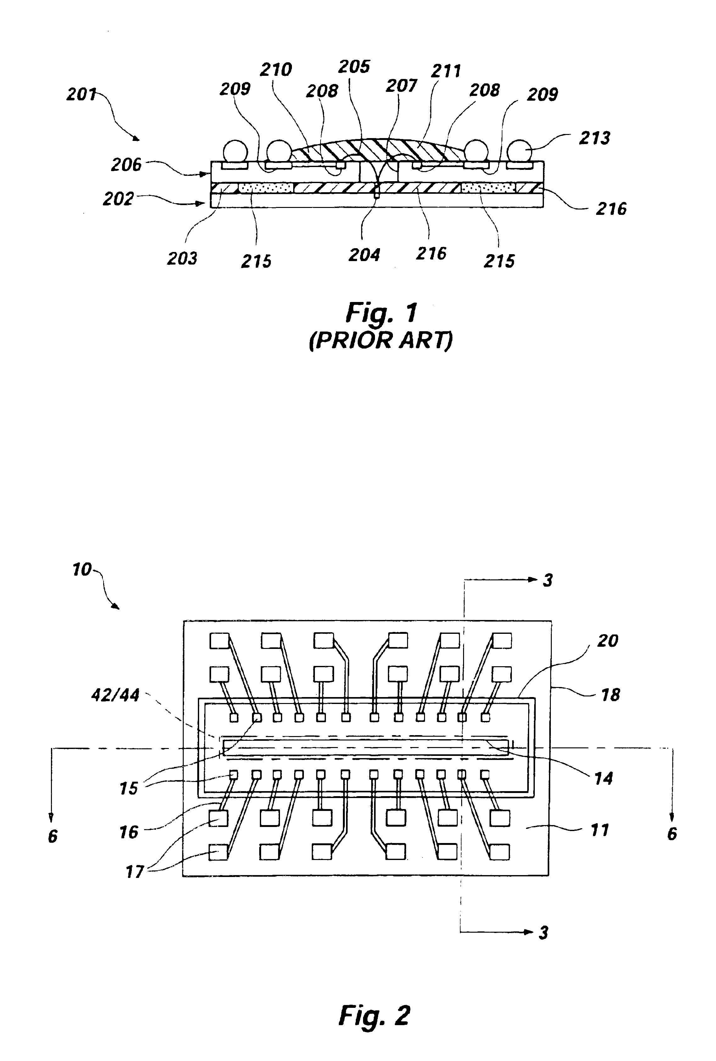
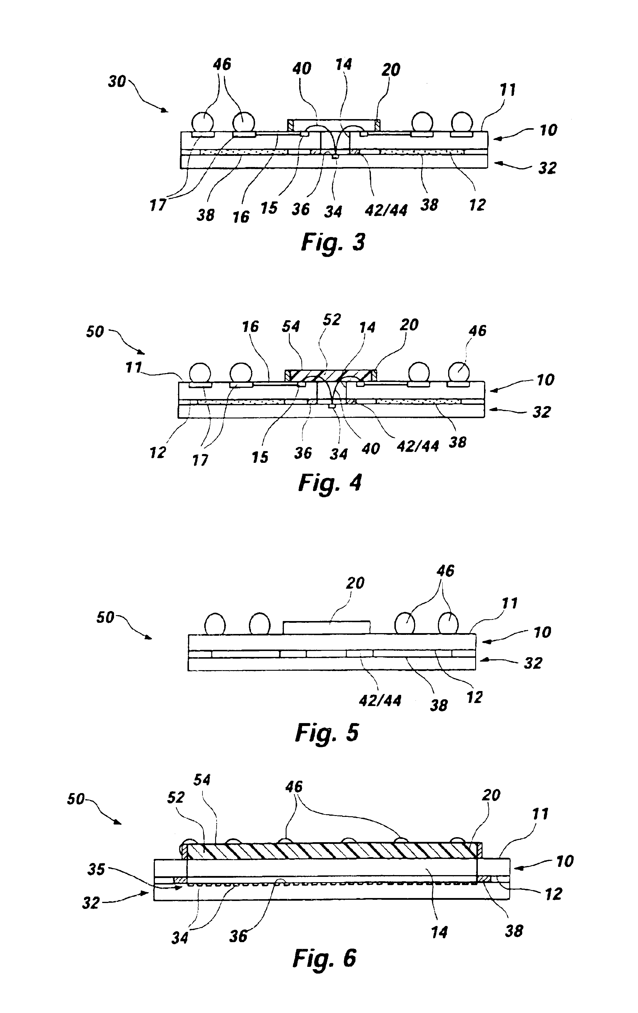
[0053]With reference to FIG. 2, an exemplary interposer 10 incorporating teachings of the present invention is shown. Interposer 10 is a substantially planar member formed from, for example, FR-4 resin, semiconductor material (e.g., silicon), or any other known substrate material and having an upper surface 11 and a lower surface 12 (see FIGS. 2-6). As illustrated in FIG. 2, interposer 10 includes an elongate slot 14 formed therethrough. Slot 14 is positioned substantially along the center of interposer 10. Interposer 10 also includes first contact pads 15, or contacts, located proximate slot 14. Electrical traces 16 carried by interposer 10 connect each first contact pad 15 to a corresponding second contact pad 17 carried on upper surface 11 of interposer 10. As depicted, second contact pads 17 are arranged in an array over upper surface 11.

[0054]A dam 20 secured to upper surface 11 of interposer 10 protrudes upwardly therefrom. Dam 20 at least partially laterally surrounds slot 14...


PUM


Abstract

A method for fabricating an interposer includes providing an interposer substrate with at least one slot or aperture therethrough and forming at least one upwardly protruding dam on the interposer substrate, adjacent to the slot or aperture. The upwardly protruding dam or dams may at least partially surround the slot or aperture. Accordingly, the upwardly protruding dam or dams may laterally confine encapsulant material over the slot or aperture and over any intermediate conductive elements extending through the slot or aperture. Programmed material consolidation processes, such as stereolithography, may be used to form the at least one upwardly protruding dam.

Description

CROSS-REFERENCE TO RELATED APPLICATIONS[0001]This application is a divisional of application Ser. No. 10 / 301,385, filed Nov. 21, 2002, which is a continuation of application Ser. No. 09 / 560,970, filed Apr. 28, 2000, now U.S. Pat. No. 6,531,335, issued Mar. 11, 2003.BACKGROUND OF THE INVENTION[0002]1. Field of the Invention[0003]The present invention relates generally to interposers for use in chip-scale packages (CSPs), including ball grid array (BGA) packages. Particularly, the present invention relates to interposers that include upwardly protruding dams configured to laterally confine encapsulant material over a specified area of the interposer. The invention also relates to semiconductor device packages including the interposers and to methods of fabricating the upwardly protruding dams, the interposers, and assemblies including the interposers.Semiconductor Device Packages[0004]2. Background of Related Art[0005]Semiconductor devices, such as memory devices and processors, are g...

Claims


Application Information

Patent Timeline
IPC IPC(8): H01L21/44H01L21/48H01L21/50H01L23/24H01L23/31H01L23/498
CPCH01L23/24H01L23/49816H01L23/3107H01L2224/73215H01L2224/32225H01L2924/01087H01L24/48H01L2924/15311H01L2924/01039H01L2224/4824H01L2224/16H01L2924/00012H01L2924/12042H01L2224/05599H01L2224/85399H01L2924/00014H01L2924/181B33Y80/00B33Y10/00B33Y30/00H01L2924/00H01L2224/45099H01L2224/45015H01L2924/207H01L21/44
Inventor GRIGG, FORD B.
Owner MICRON TECH INC
Why Eureka
Try Eureka