Light emitting apparatus and method for manufacturing the same

a technology of light-emitting apparatus and manufacturing method, which is applied in the direction of thermoelectric devices, organic semiconductor devices, transistors, etc., can solve the problems of difficult to form determined patterns on the organic electro-luminescence layer, degraded alkali metal or alkali earth metal used for an electrode, and narrow angled field of view, so as to improve the reliability of the light-emitting apparatus

Inactive Publication Date: 2006-05-09
SEMICON ENERGY LAB CO LTD
View PDF42 Cites 102 Cited by
  • Summary
  • Abstract
  • Description
  • Claims
  • Application Information

AI Technical Summary

Benefits of technology

[0012]The purpose of the present invention is to solve the above problems in order to improve the reliability of a light emitting apparatus comprising TFTs and organic light emitting elements.
[0014]The silicon nitride film manufactured by the RF sputtering has improved effect of blocking the external impurities and an effect of suppressing the deterioration of the light emitting element by satisfying one of the following conditions; (1) a silicon nitride film with etching rate of 9 nm / min or less (preferably, 0.5 to 3.5 nm / min or less), (2) hydrogen concentration of 1×10²¹ atoms / cm3 or less (preferably 5×10²⁰ atoms / cm3 or less), (3) hydrogen concentration of 1×10²¹ atoms / cm3 or less (preferably 5×10²⁰ atoms / cm3 or less), and oxygen concentration from 5×10¹⁸ to 5×10²¹ atoms / cm3 (preferably 1×10¹⁹ to 1×10²¹ atoms / cm3), (4) etching rate of 9 nm / min or less (preferably, 0.5 to 3.5 nm / min or less), and hydrogen concentration of 1×10²¹ atoms / cm3 or less (preferably 5×10²⁰ atoms / cm3 or less), or (5) etching rate of 9 nm / min or less (preferably, 0.5 to 3.5 nm / min or less), hydrogen concentration of 1×10²¹ atoms / cm3 or less (preferably 5×10²⁰ atoms / cm3 or less), and oxygen concentration from 5×10¹⁸ to 5×10²¹ atoms / cm3 (preferably 1×10¹⁹ to 1×10²¹ atoms / cm3).
[0015]In a construction wherein a display screen has light emitting elements arranged in matrix, the most preferable construction of an insulation layer to partition the each pixel comprises a positive-type or a negative-type photosensitive organic resin material and has a curvature radius of 0.2 to 2 μm or continuously varying curvature radiuses within the above range at the end of the patterns, and a tapered surface with an inclination angle from 10 to 75 degrees, preferably from 35 to 45 degrees. The construction of a pixel in the light emitting apparatus according to the invention can mitigate the stress on the electrode ends of the pixel and suppress the deterioration of the light emitting element, by forming an insulation layer which covers ends of the individual electrode (either anode or cathode) of each pixel connecting to the TFT to partition each pixel, and by forming a layer containing the light emitting material, and one of the anode layer or the cathode layer, from over the pixel electrode to over the insulation layer.
[0043]The third to the fifth inorganic insulation layers have the above mentioned etching characteristics, and hydrogen concentration and oxygen concentration in the above range. By reducing the density of N—H bond, Si—H bond and the Si—O bond, the construction according to the invention can improve thermal stability of a film and make a fine film.

Problems solved by technology

A liquid crystal display apparatus is employed as an image displaying unit in various electronics, but suffers a structural problem that it has a narrow angled field of view.
However, it is difficult to form determined patterns on the organic electro-luminescence layer by photolithography technique as used in the semiconductor element manufacturing.
In the first place, It was pointed out as a problem that an organic compound used for the light emitting elements, and an alkali metal or an alkali earth metal used for an electrode are degraded by reactions with water and oxygen.
When the organic compound has low melting point or glass transition temperature, the electric field concentrates around pinholes or cracks and dielectric breakdown occur.
Almost no organic compound can keep its amorphous structure for a long time.
Furthermore, the crack or the break may lead to a progressive defect such as dark spots.
However in practice, the deterioration is caused by two or more of the above factors, which makes it difficult to take effective preventive measure.
Unfortunately, conventional preventive measures have failed to suppress the deterioration of the light emitting apparatus to an acceptable level.

Method used


Image

  • Light emitting apparatus and method for manufacturing the same
  • Light emitting apparatus and method for manufacturing the same
  • Light emitting apparatus and method for manufacturing the same

Examples


embodiments

Embodiment 1

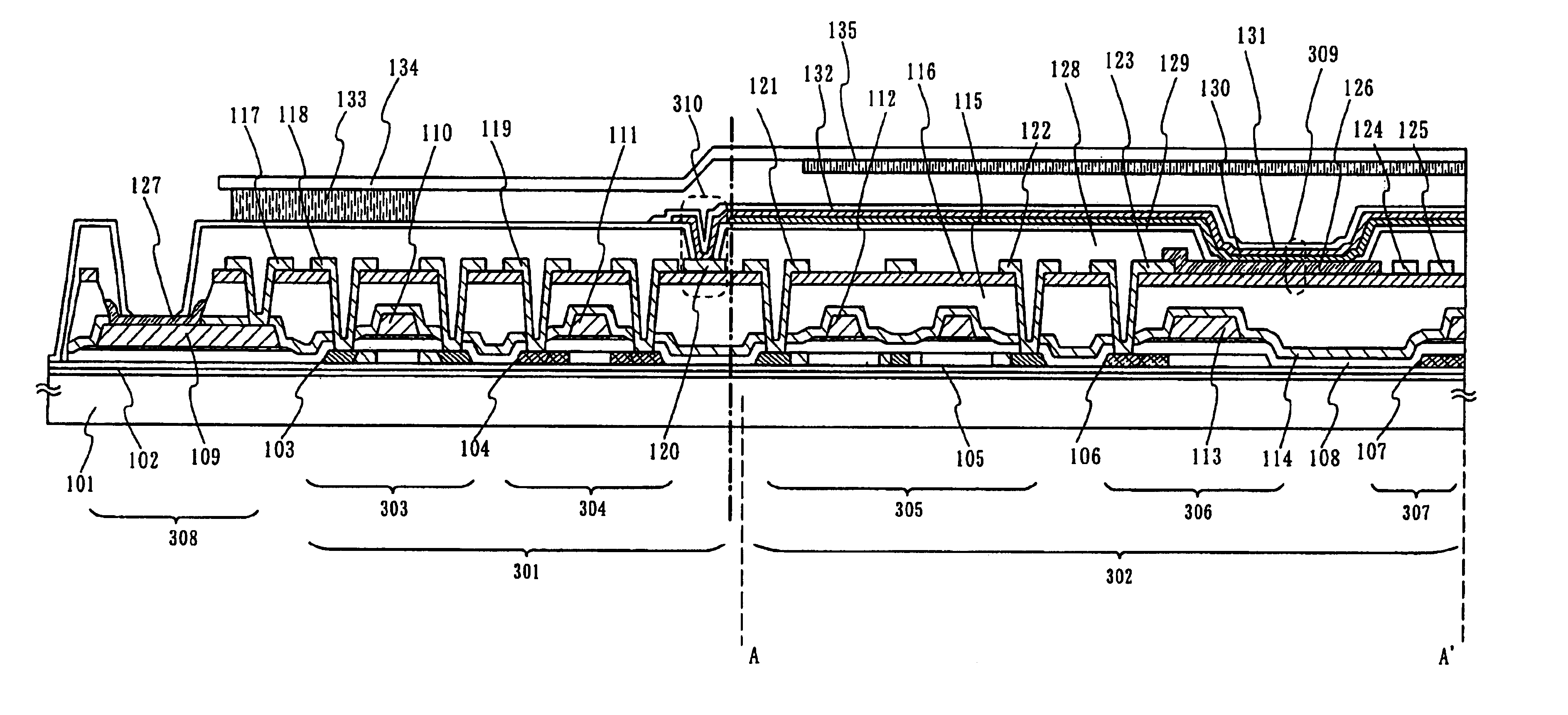
[0166]Next, the process of manufacturing the light emitting apparatus shown in FIG. 1 is described with reference to the figures.

[0167]In FIG. 8A, the substrate 101 maybe one of a glass substrate, a quartz substrate or a ceramic substrate. The substrate 101 may comprise a silicon substrate, a metal substrate or a stainless substrate with an insulation layer formed thereon. A plastic substrate having heat resistance bearable to the processing temperature of the embodiment is acceptable.

[0168]A first inorganic insulation layer 102 consisting of an insulation film such as a silicon oxide film, a silicon nitride film or a silicon oxynitride film (SiOxNy) is formed on the substrate 101. A typical example has a two-layer construction, in which the first silicon oxynitride film of 50 nm thickness is formed using SiH4, NH3 and N2O as reaction gases, and the second silicon oxynitride film of 100 nm thickness is formed on the first film, using SiH4 and N2O as reaction gases.

[0169]...

embodiment 2

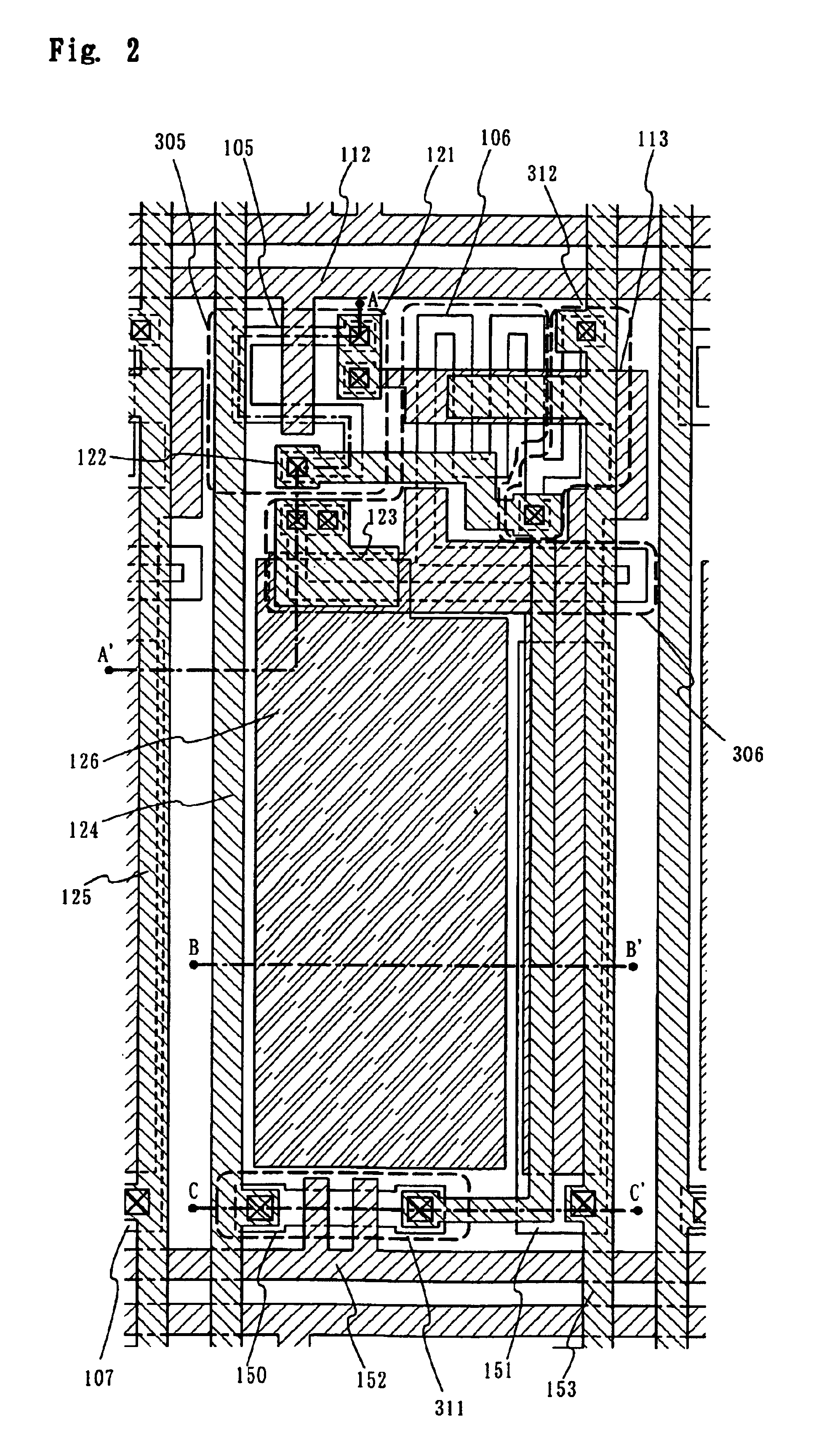
[0192]This embodiment has a different construction than that of the embodiment 1 for the pixel section, as illustrated in FIGS. 31 and 32. In this embodiment, the processes from the beginning to the formation of the third inorganic insulation layer 116 wiring 123, and anode 126 are same as FIG. 1.

[0193]As shown in FIG. 31A, a second organic insulation layer 180 covering the end of the anode 126 is formed of a photosensitive, negative-type acrylic resin. Thus, the end where the second organic insulation layer 180 contacts with the anode 126 has a inclined surface having a curvature as shown in Figure, the shape of which can be expressed by at least two curvatures R1 and R2. The center of the R1 is located above the wiring, while that of the R2 is located below the wiring. This shape may vary slightly depending on the exposure, but the thickness of the film is 1.5 μm and the value for R1 and R2 is 0.2 to 2 μm. The inclined surface has continuously varying curvatures.

[0194]Then, along ...

embodiment 3

[0197]For the embodiments 1 to 2, there is no restriction on the construction of the organic compound layer in the light emitting element 309, so that, any known construction is applicable. The organic compound layer 130 has a light emitting layer, a positive holes injecting layer, an electrons injecting layer, a positive holes transferring layer and an electrons transferring layer, and may have a construction wherein these layers are laminated, or a construction wherein a part or all of the materials forming these layers are mixed. Particularly, the light emitting layer, the positive holes injecting layer, the electrons injecting layer, the positive holes transferring layer and the electrons transferring layer are included. A basic EL element has a construction wherein an anode, a light emitting layer, a cathode are laminated in this order. Other possible construction includes a construction wherein the layers are laminated in an order of an anode, a positive holes injection layer,...


PUM


Abstract

The purpose of the invention is to improve reliability of a light emitting apparatus comprising TFTs and organic light emitting elements. The light emitting apparatus according to the invention having thin film transistors and light emitting elements, comprises; a second inorganic insulation layer on a gate electrode, a first organic insulation layer on the second inorganic insulation layer, a third inorganic insulation layer on the first organic insulation layer, an anode layer formed on the third inorganic insulation layer, a second organic insulation layer overlapping with the end of the anode layer and having an inclination angle of 35 to 45 degrees, a fourth inorganic insulation layer formed on the upper surface and side surface of the second organic insulation layer and having an opening over the anode layer, an organic compound layer formed in contact with the anode layer and the fourth inorganic insulation layer and containing light emitting material, and a cathode layer formed in contact with the organic compound layer containing the light emitting material, wherein the third inorganic insulation layer and the fourth inorganic insulation layer are formed with silicon nitride or aluminum nitride.

Description

BACKGROUND OF THE INVENTION[0001]1. Field of the Invention[0002]The present invention relates to a light emitting apparatus comprising a light emitting element which emits fluorescent light or phosphorescent light. In particular, the invention relates to a light emitting apparatus comprising an active element such as insulation gate type transistor or a TFT, and a light emitting element coupled thereto.[0003]2. Description of the Related Art[0004]A typical display apparatus utilizing liquid crystal uses a back light or a front light for displaying images. A liquid crystal display apparatus is employed as an image displaying unit in various electronics, but suffers a structural problem that it has a narrow angled field of view. On the contrary, a display which uses light emitting elements providing electro-luminescence as a display unit has a wider-angled field of view as well as high level of visual recognition. These advantages make the electro-luminescent display prospective for t...

Claims


Application Information

Patent Timeline
Patent Type & Authority Patents(United States)
IPC IPC(8): H01L29/24H01L33/00H01L21/336H01L21/77H01L21/84H01L27/12H01L27/32H01L29/786H01L51/56
CPCH01L27/3244H01L29/78621H01L29/66757H01L29/78645H01L27/1248H01L51/5237H01L27/12H01L27/3246H01L2227/323H01L27/3258H01L51/56H01L51/5008H01L2251/566H10K59/122H10K59/124H10K59/12H10K30/865H10K50/841H10K50/844H10K59/1201H10K71/851H10K71/00H01L29/16H01L29/78675H01L29/78696
Inventor YAMAZAKI, SHUNPEIMURAKAMI, SATOSHISAKAKURA, MASAYUKITAKAYAMA, TORU
Owner SEMICON ENERGY LAB CO LTD
Why Eureka
Try Eureka