Semiconductor device of reduced gate overlap capacitance and method of manufacturing the semiconductor device

a semiconductor device and semiconductor technology, applied in the field of semiconductor devices, can solve the problems of increasing the difficulty of reducing the gate overlap length in proportion to the gate length, the inability to reduce so as to achieve the effect of reducing the gate overlap capacitan

Inactive Publication Date: 2006-05-16
RENESAS ELECTRONICS CORP
View PDF13 Cites 4 Cited by
  • Summary
  • Abstract
  • Description
  • Claims
  • Application Information

AI Technical Summary

Benefits of technology

[0010]It is an object of the present invention to provide an MOS transistor capable of reducing gate overlap capacitance without decreasing the driving current of the MOS transistor.

Problems solved by technology

As the channel length of an MOS transistor is decreased with increasing the integration degree of semiconductor integrated circuits, it is increasingly difficult to reduce a gate overlap length in proportion to a gate length.
However, a reduction in gate overlap capacitance cannot be achieved only by increasing both ends of a gate oxide film and even a problem such as reduction in driving current may occur.

Method used


Image

  • Semiconductor device of reduced gate overlap capacitance and method of manufacturing the semiconductor device
  • Semiconductor device of reduced gate overlap capacitance and method of manufacturing the semiconductor device
  • Semiconductor device of reduced gate overlap capacitance and method of manufacturing the semiconductor device

Examples


Embodiment Construction

A. First Preferred Embodiment

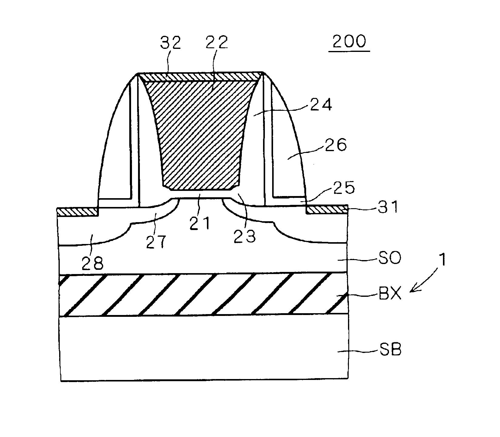
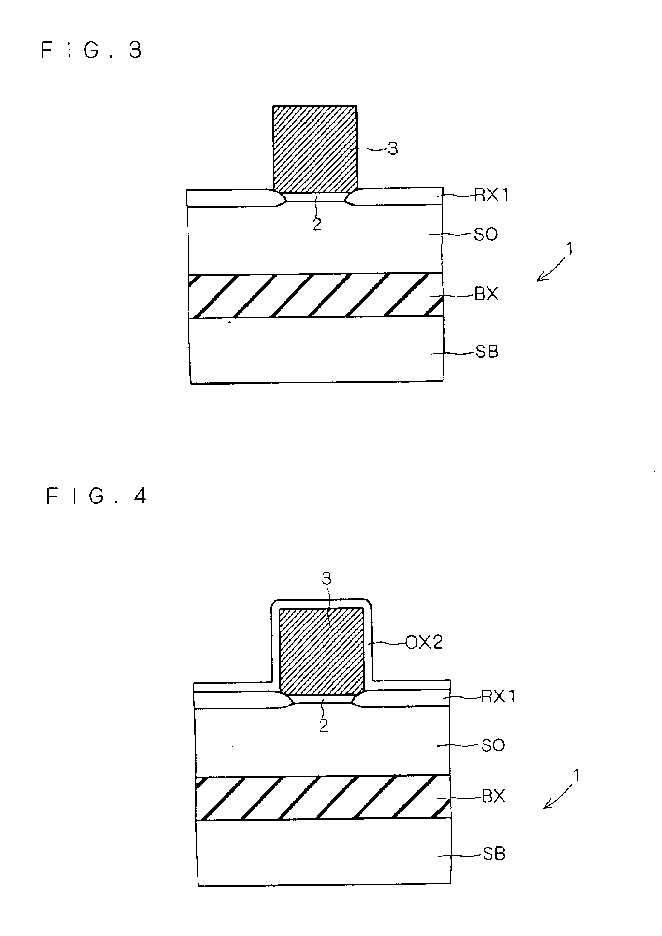
[0026]First, a method of manufacturing an MOS transistor 100 according to a first preferred embodiment of the present invention will be described with reference to FIGS. 1 to 7, sequentially showing its manufacturing steps. The configuration of the MOS transistor 100 is plotted in FIG. 7 showing the final step.

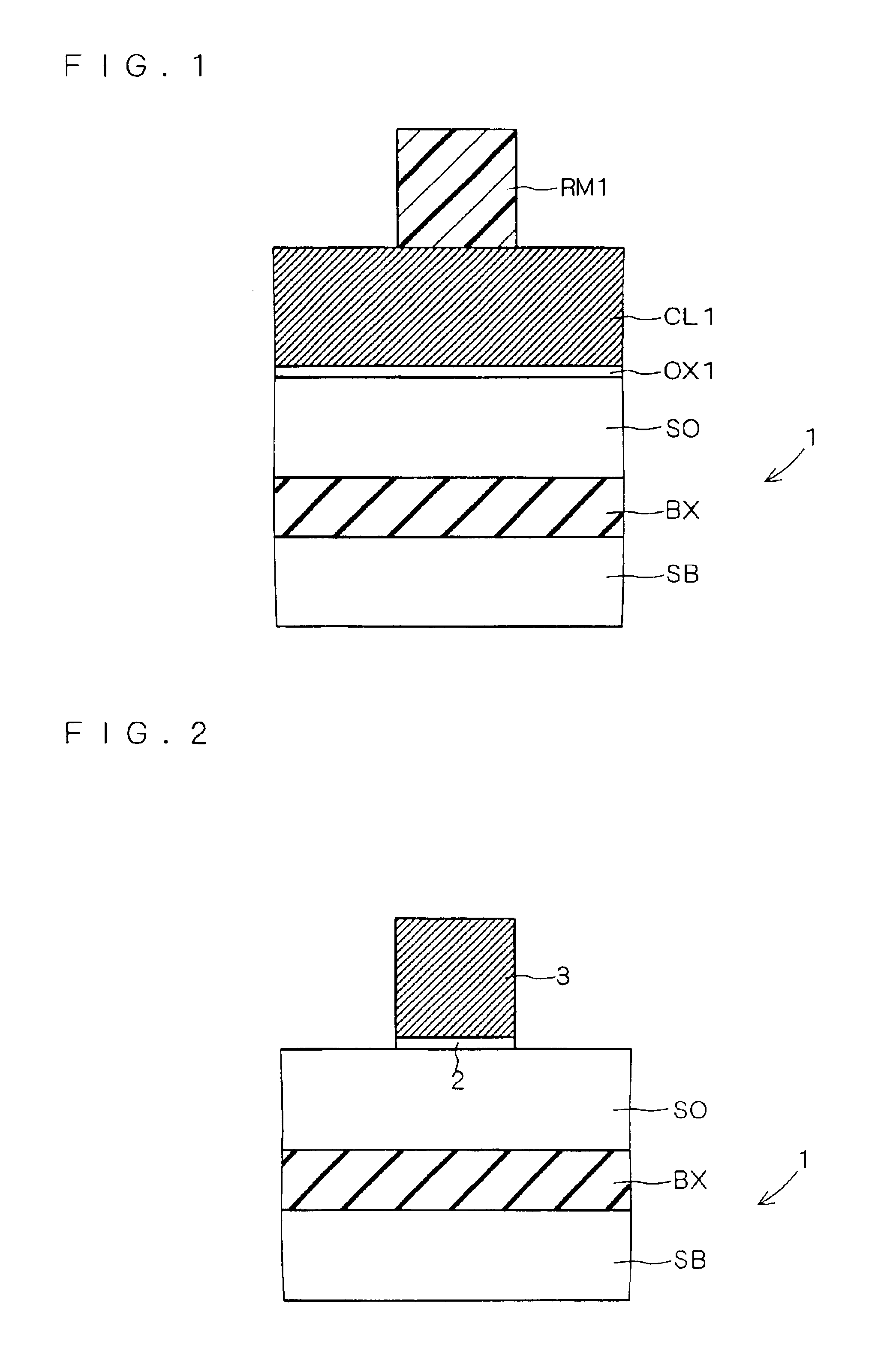
[0027]Referring now to FIG. 1, an SOI substrate 1 configured by a silicon substrate SB, buried oxide film BX, and SOI layer SO is prepared. Then, a silicon oxide film OX1 having a thickness of 1 to 4 nm is formed on the entire surface of a main surface of the SOI layer SO, by for example thermal oxidation, radical oxidation, radical nitriding method or a combination of these. The silicon oxide film OX1 will be used later as a gate oxide film (gate insulating film). Instead of the silicon oxide film, a silicon nitride film may be used to form the gate insulating film.

[0028]Thereafter, a conductive film CL1 having a thickness of 50 to 200 nm is forme...


PUM


Abstract

Provided is an MOS transistor capable of reducing gate overlap capacitance without decreasing the driving current of the MOS transistor. Specifically, a double-angle smile oxidation structure is obtainable by curving the side surface of a gate electrode (22) so as to widen upwardly, and thickening the edge portion of a gate oxide film (21) by re-oxidation. The impurity concentration of a source/drain layer under the double-angle smile oxidation structure (a region around point B) is set to the range of 4×1018 cm−3±40%.

Description

BACKGROUND OF THE INVENTION[0001]1. Field of the Invention[0002]The present invention relates to a semiconductor device and its manufacturing method. In particular, the present invention relates to a semiconductor device of reduced gate overlap capacitance and a method of manufacturing the semiconductor device.[0003]2. Description of the Background Art[0004]As the channel length of an MOS transistor is decreased with increasing the integration degree of semiconductor integrated circuits, it is increasingly difficult to reduce a gate overlap length in proportion to a gate length. As the result, the rate of gate overlap capacitance to intrinsic gate capacitance is greatly increased.[0005]A reduction in parasitic capacitance, especially gate overlap capacitance, is the key to achieve high-speed operation of transistors at low power supply voltages.[0006]As a technique of reducing gate overlap capacitance, there is one in which an already formed gate oxide film is further oxidized to in...

Claims


Application Information

Patent Timeline
Patent Type & Authority Patents(United States)
IPC IPC(8): H01L29/76H01L29/423H01L21/336H01L29/45H01L29/49H01L29/78H01L29/786
CPCH01L29/78621H01L29/66772H01L29/4908H01L29/458H01L29/78
Inventor DANG, HAIMAEDA, SHIGENOBUMATSUMOTO, TAKUJIHIRANO, YUUICHI
Owner RENESAS ELECTRONICS CORP
Why Eureka
Try Eureka