Using hole- or electron-blocking layers in color OLEDS

a color oled, electron-blocking technology, applied in the manufacture of electrode systems, electric discharge tubes/lamps, discharge tubes luminescnet screens, etc., can solve the problems of adding to the time and complexity of manufacture, and achieve the effect of reducing the number of alignment and patterned transfer steps, reducing the number of handling steps, and simplifying the manufacturing process of color oled devices

Inactive Publication Date: 2006-05-30
GLOBAL OLED TECH
View PDF17 Cites 26 Cited by
  • Summary
  • Abstract
  • Description
  • Claims
  • Application Information

AI Technical Summary

Problems solved by technology

In all these methods one patterned transfer is necessary per color adding to the time and complexity of manufacture.

Method used


Image

  • Using hole- or electron-blocking layers in color OLEDS
  • Using hole- or electron-blocking layers in color OLEDS
  • Using hole- or electron-blocking layers in color OLEDS

Examples


example 1 (

INVENTIVE EXAMPLE)

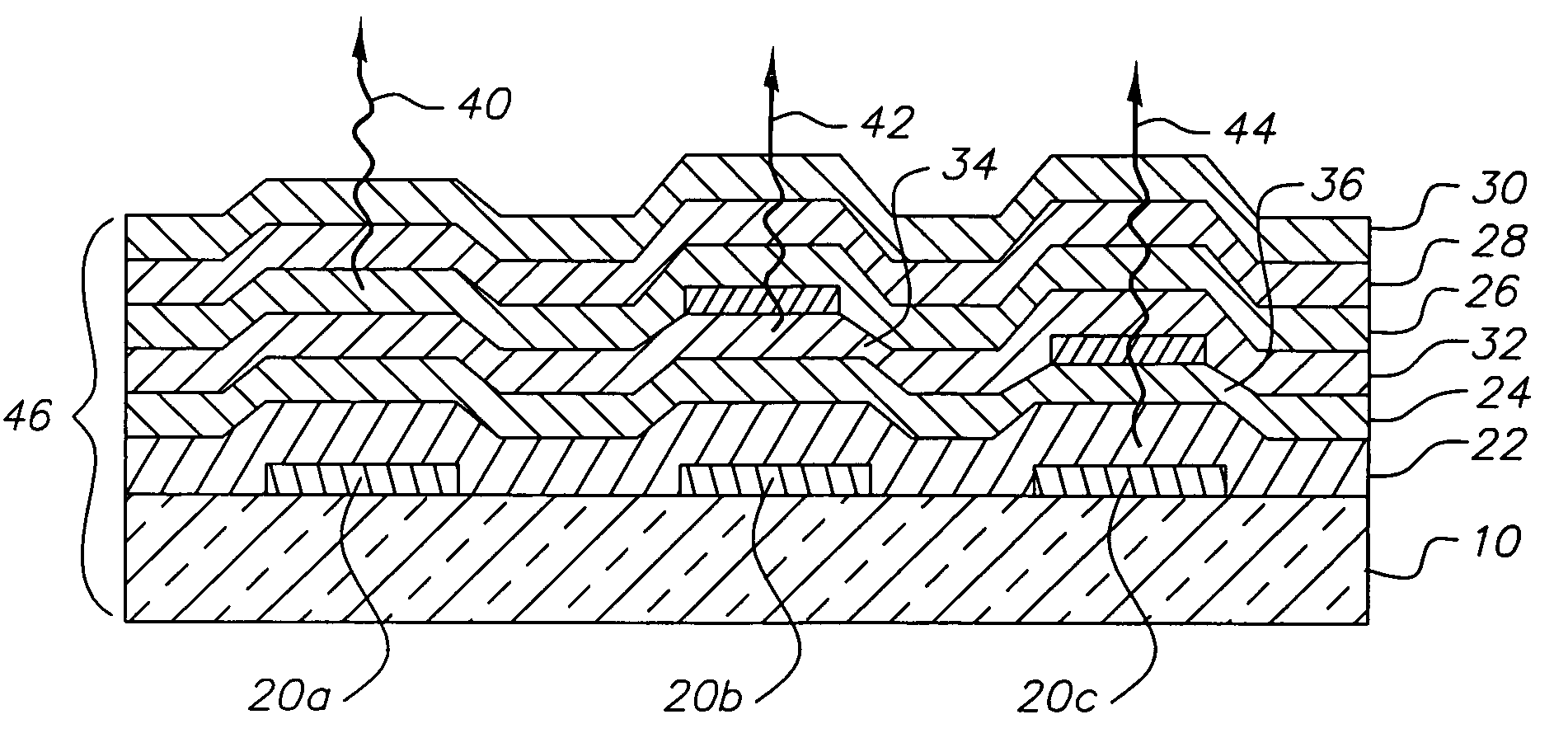
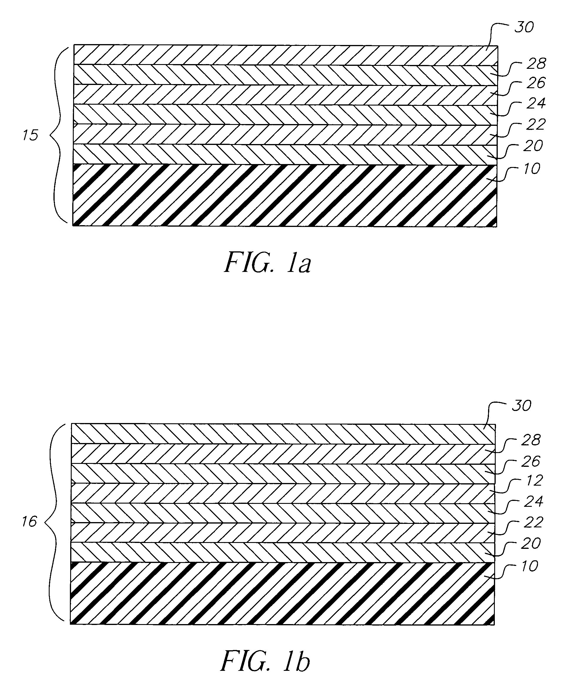
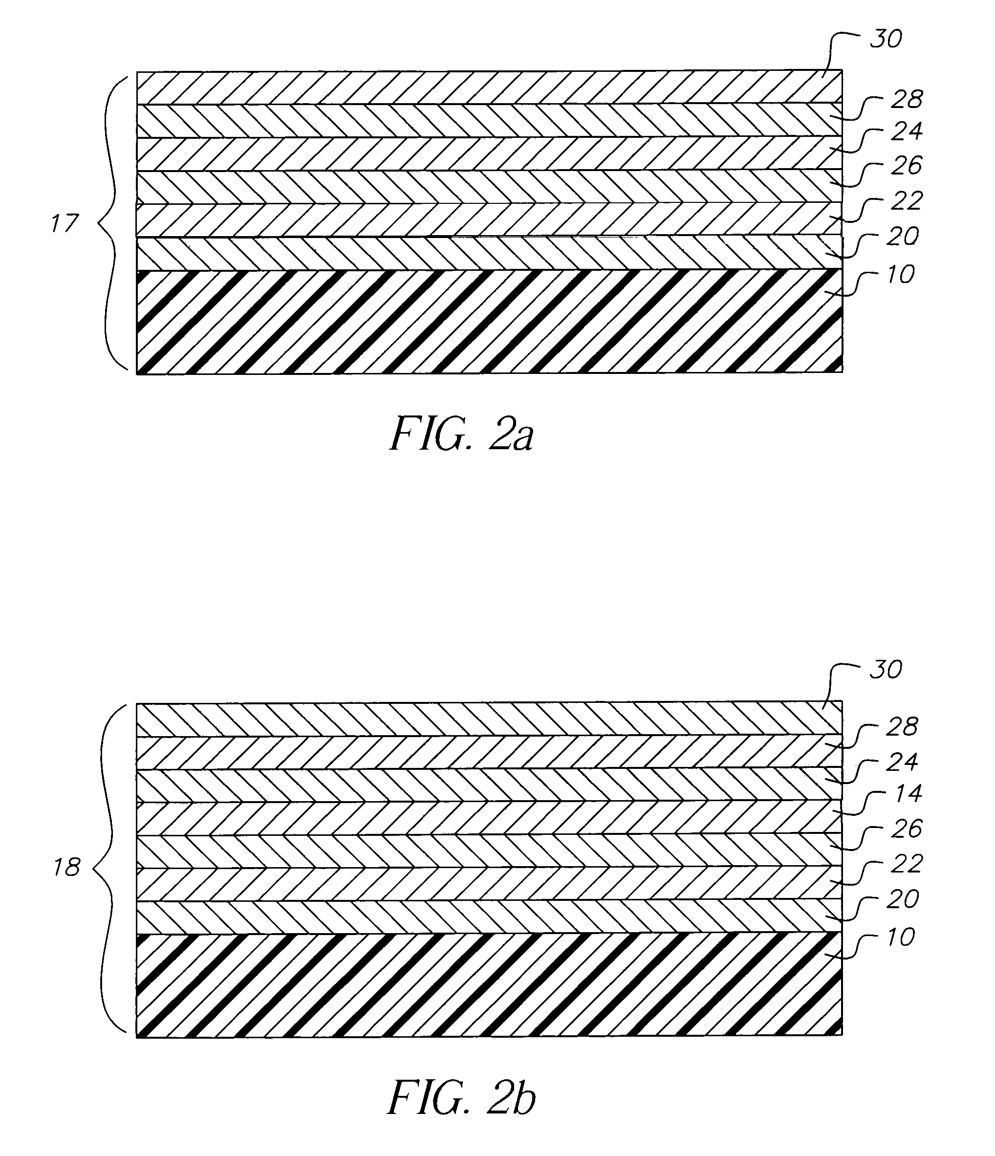
[0148]An OLED device with an electron-blocking layer satisfying the requirements of the invention was constructed in the following manner.

1. A clean glass substrate was vacuum-deposited with indium tin oxide (ITO) through a mask to form a pattern of transparent electrodes of 40 to 80 nm thickness.

2. The above-prepared ITO surface was treated with a plasma oxygen etch, followed by plasma deposition of a 0.1 nm layer of a fluorocarbon polymer (CFx) as described in U.S. Pat. No. 6,208,075.

[0149]3. The above-prepared substrate was further treated by vacuum-depositing a 40 nm layer of 4,4′-bis[N-(1-naphthyl)-N-phenylamino]biphenyl (NPB) as a hole-transporting layer followed by a 15.3 nm layer of of 2-tert-butyl-9,10-bis(2-naphthyl)anthracene (TBADN) with 2% 4-(dicyanomethylene)-2-t-butyl-6-(1,1,7,7-tetramethyljulolidyl-9-enyl)-4H-pyran (DCJTB) (a red dopant).

4. A coating of 30 nm of 1,1-bis(4-di-p-tolylaminophenyl)cyclohexane (TAPC) as the electron blocker was evaporati...

example 3 (

INVENTIVE EXAMPLE)

[0152]An OLED device with an electron-blocking layer satisfying the requirements of the invention was constructed in the manner described in Example 1, except Step 3 was performed as follows:

[0153]3. The above-prepared substrate was further treated by vacuum-depositing a 40 nm layer of 4,4′-bis[N-(1-naphthyl)-N-phenylamino]biphenyl (NPB) as a hole-transport layer followed by a 20.4 nm layer of of ALQ with 2% 4-(dicyanomethylene)-2-t-butyl-6-(1,1,7,7-tetramethyljulolidyl-9-enyl)-4H-pyran (DCJTB) (a red dopant).

example 5 (

INVENTIVE EXAMPLE)

[0155]An OLED device with an electron blocker deposited by laser thermal transfer and satisfying the requirements of the invention was constructed in the following manner.

1. Onto a polyimide donor support element film having a thickness of 104 microns, a coating of 60 nm of chromium metal was evaporatively deposited.

2. A further coating of 30 nm of TAPC was evaporatively deposited on the above donor support element.

3. A clean glass substrate was vacuum-deposited with indium tin oxide (ITO) through a mask to form a pattern of transparent electrodes of 40 to 80 nm thickness.

4. The above-prepared ITO surface was treated with a plasma oxygen etch, followed by plasma deposition of a 0.1 nm layer of a fluorocarbon polymer (CFx) as described in U.S. Pat. No. 6,208,075.

[0156]5. The above-prepared substrate was further treated by vacuum-depositing a 40 nm layer of 4,4′-bis[N-(1-naphthyl)-N-phenylamino]biphenyl (NPB) as a hole-transporting layer followed by a 30.6 nm layer o...


PUM

PropertyMeasurementUnit
work functionaaaaaaaaaa
wavelengthsaaaaaaaaaa

Abstract

A method for forming a color organic light-emitting device including depositing a first electrode over a substrate; depositing a first emissive layer over the first electrode for producing a first colored light in response to hole-electron recombination; and selectively patternwise depositing a hole-blocking layer over the first emissive layer. The method also includes depositing a second emissive layer over the hole-blocking layer which in response to hole-electron recombination emits colored light different from the colored light emitted from the first emissive layer; depositing a second electrode over the second emissive layer; and whereby the patternwise deposition of the hole-blocking layer has been selected to substantially shift hole-electron recombination from the second to the first emissive layers.

Description

CROSS REFERENCE TO RELATED APPLICATIONS[0001]Reference is made to commonly assigned U.S. patent application Ser. No. 10 / 055,579 filed Jan. 23, 2002 by David B. Kay et al., entitled “Using a Multichannel Linear Laser Light Beam in Making OLED Devices by Thermal Transfer”, the disclosure of which is herein incorporated by reference.FIELD OF THE INVENTION[0002]The present invention relates to color organic electroluminescent (EL) devices, also known as color organic light-emitting diodes (OLED), and more particularly to an OLED that has at least two emissive layers, which emit different color light.BACKGROUND OF THE INVENTION[0003]In color or full-color organic electroluminescent (EL) displays (also known as organic light-emitting diode devices, or OLED devices) having an array of colored pixels such as red, green, and blue color pixels (commonly referred to as RGB pixels), precision patterning of the color-producing organic EL media are required to produce the RGB pixels. The basic OL...

Claims


Application Information

Patent Timeline
Patent Type & Authority Patents(United States)
IPC IPC(8): H05B33/10H01L27/32H01L51/00H01L51/30H01L51/50
CPCH01L27/3211H01L51/5096H01L51/0052H01L51/0059H01L51/0062H01L51/0081H01L51/0084H01L51/0085H01L51/0089H01L51/0077H10K59/35H10K85/615H10K85/649H10K85/631H10K85/30H10K85/341H10K85/351H10K85/324H10K85/342H10K50/18
Inventor TUTT, LEE W.KONDAKOV, DENIS Y.CULVER, MYRON W.
Owner GLOBAL OLED TECH
Why Eureka
Try Eureka