Bonded substrate for an integrated circuit containing a planar intrinsic gettering zone

a technology of intrinsic gettering and bonded substrates, which is applied in the field of gettering, can solve the problems of stacking faults, affecting the yield of final products, and reducing the performance or reliability of final products, so as to facilitate small geometry manufacturing, improve the efficiency of contaminant removal, and ensure the effect of construction

Inactive Publication Date: 2006-05-30
INTERSIL INC
View PDF11 Cites 6 Cited by
  • Summary
  • Abstract
  • Description
  • Claims
  • Application Information

AI Technical Summary

Benefits of technology

[0017]The bonded substrate of the present invention includes a narrowly restricted gettering zone located in near proximity to device regions, which increases the efficiency of contaminant removal from those regions and facilitates small geometry manufacture. Because the gettering zone comprises substantially pure semiconductor material, its formation affects only the structural characteristics and not the electrical characteristics of the wafer. The bonded substrate of the invention is reliably constructed and provides excellent structural stability to devices formed on it over a wide range of processing temperature and conditions.

Problems solved by technology

During integrated circuit manufacture and processing, a silicon wafer may be exposed to metallic contaminants such as iron, nickel, zinc, chrormium, and the like that may ultimately degrade the final product yield, performance, or reliability.
This contamination may occur through contact with stainless steel wafer handlers and tools, diffusion of metallic substances from beater coils or lamps in high temperature processing chambers, or sputter debris dislodging from plasma chamber walls.
Extrinsic gettering entails the use of external means (usually on the wafer back surface) to create damage or stress in the silicon lattice, leading to the creation of extended defects capable of mobile metal capture.
The stresses resulting from the agglomerate clusters cause stacking faults and dislocation loops that are capable of trapping impurities.
However the defects are distributed vertically throughout the layer, extending even to the exterior surface, where they may adversely affect bonding of the layer with other layers.
In addition, grinding and polishing of the layer results in substantial loss of the gettering sites.
Commonly employed gettering techniques are inadequate for use with many desired semiconductor devices.
For example, the formation of gettering sites by treatment of the back surface of a device is generally unsuited for application to semiconductor-on-insulator structures.
Also, defects that provide gettering sites are often generated in an indiscriminate, scattered fashion throughout the wafer and may thus adversely affect the performance of a device subsequently formed in the wafer.

Method used


Image

  • Bonded substrate for an integrated circuit containing a planar intrinsic gettering zone
  • Bonded substrate for an integrated circuit containing a planar intrinsic gettering zone
  • Bonded substrate for an integrated circuit containing a planar intrinsic gettering zone

Examples


Embodiment Construction

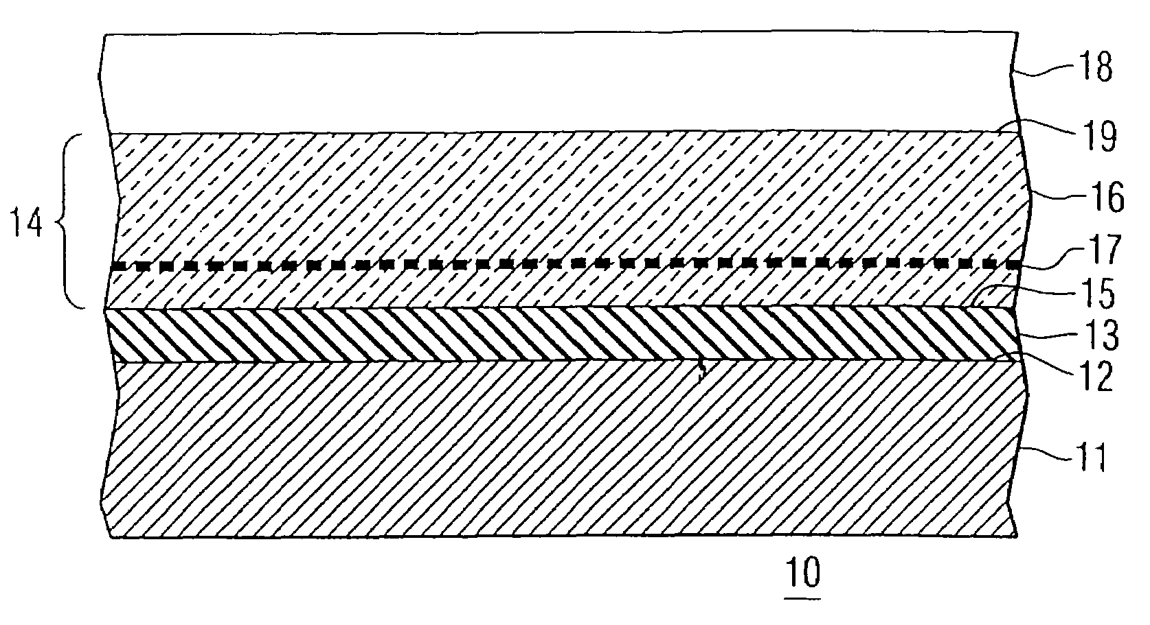
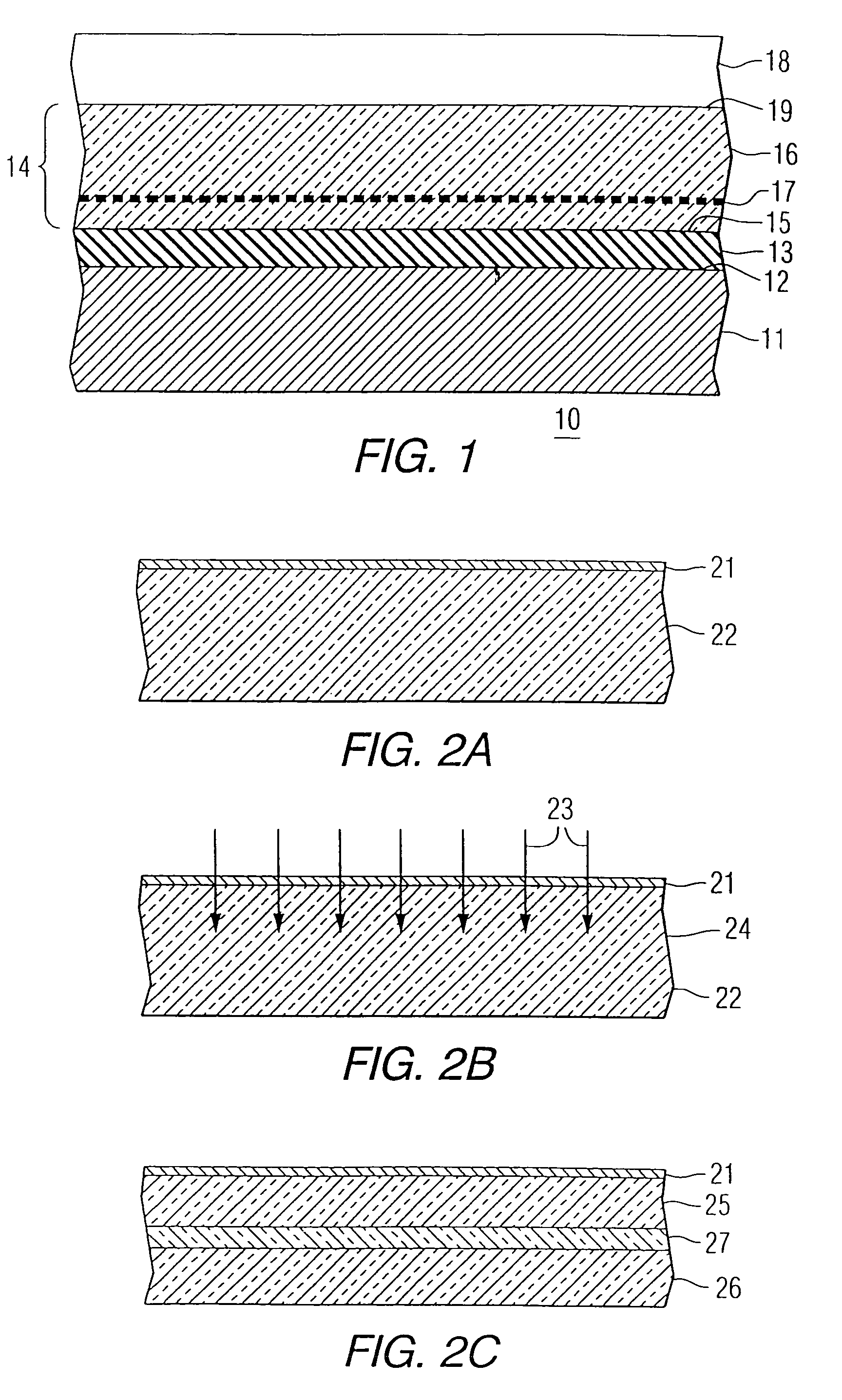
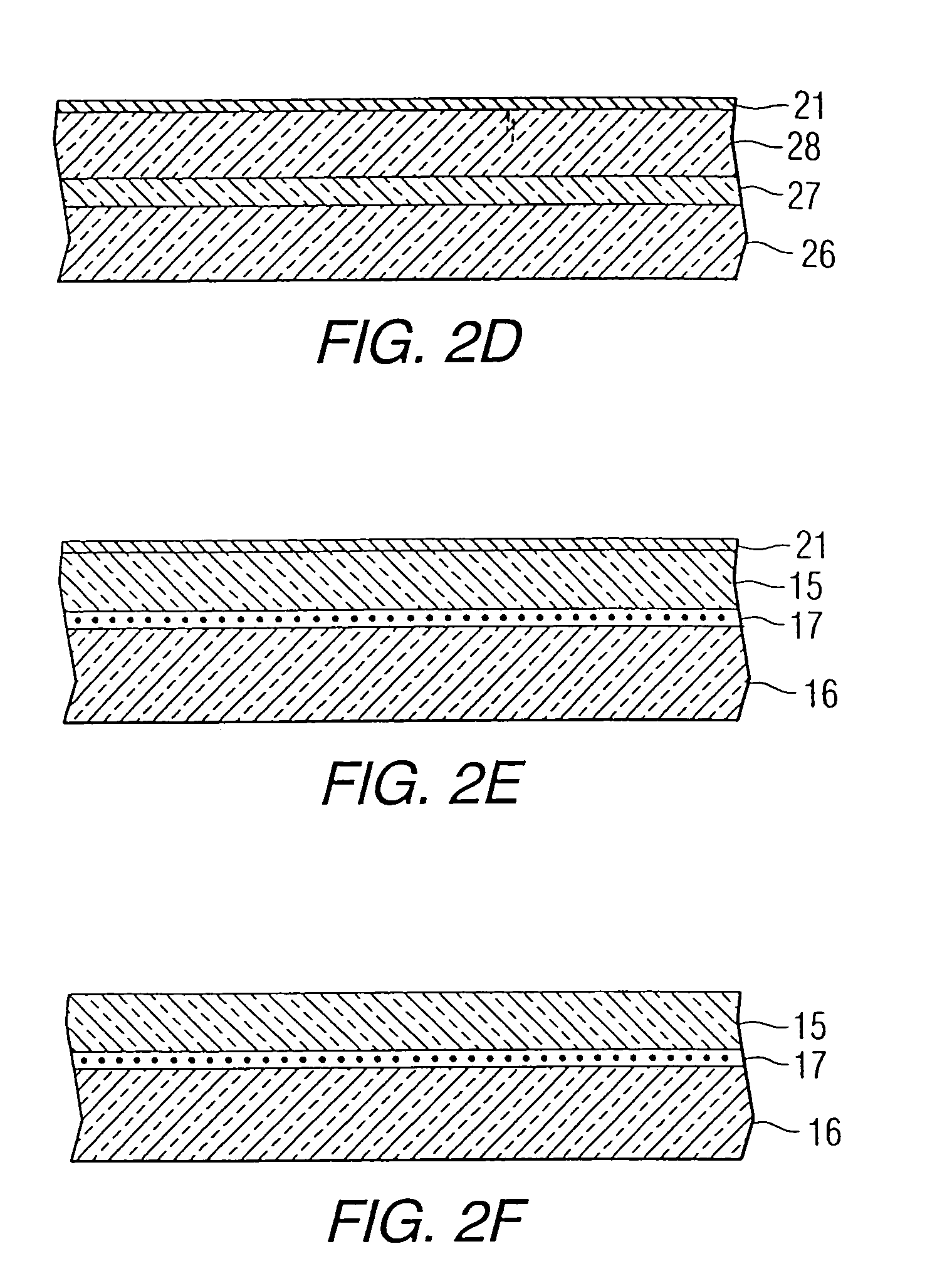
[0022]Referring to FIG. 1, a bonded substrate 10 of the present invention includes a handle wafer 11 having on one surface 12 an insulating bond layer 13 and a semiconductor device wafer 14 bonded to insulating layer 13. Semiconductor device wafer 14 has a first layer 15 of monocrystalline semiconductor material adjacent to insulating layer 13 and a second layer 16 of monocrystalline semiconductor material overlying first layer 15. Second monocrystalline semiconductor layer 16 is separated from first monocrystalline semiconductor layer 15 by an intervening substantially planar intrinsic gettering zone 17 comprising gettering sites in the monocrystalline semiconductor material. A further optional epitaxial monocrystalline semiconductor layer 18 can be deposited on surface 19 of layer 16.

[0023]FIGS. 2A–F depict the method of the invention for forming the device wafer 14 shown in FIG. 1. As depicted in FIG. 2A, an oxide layer 21 having a thickness preferably of about 1 nm to about 50 n...


PUM


Abstract

A bonded semiconductor-on-insulator substrate for an integrated circuit. The bonded semiconductor-on-insulator substrate includes a wafer, a handle wafer and an insulating bond layer. The wafer has a first layer of monocrystalline semiconductor material adjacent a first surface of the wafer. The wafer also has a second layer of undamaged by implantation monocrystalline semiconductor material adjacent a second surface of the wafer. The wafer further has a substantially planar intrinsic gettering zone of substantially pure semiconductor material and active gettering sites positioned between the first and second layers formed by implanting ions of the semiconductor material through the first layer of monocrystalline semiconductor material. The insulating bond layer bonds the handle wafer to the first surface of the wafer.

Description

CROSS REFERENCE TO RELATED APPLICATIONS[0001]This application is a continuation application of U.S. patent application Ser. No. 09 / 846,795, filed May 1, 2001 now U.S. Pat. No. 6,825,532, which is a divisional of U.S. application Ser. No. 09 / 255,231, filed Feb. 22, 1999 now U.S. Pat. No. 6,255,195.FIELD OF THE INVENTION[0002]The present invention relates to gettering in a semiconductor device and, more particularly, to a process for forming a bonded semiconductor-on-insulator substrate containing a planar intrinsic gettering zone and to a semiconductor device and an integrated circuit formed on the bonded substrate.BACKGROUND OF THE INVENTION[0003]During integrated circuit manufacture and processing, a silicon wafer may be exposed to metallic contaminants such as iron, nickel, zinc, chrormium, and the like that may ultimately degrade the final product yield, performance, or reliability. This contamination may occur through contact with stainless steel wafer handlers and tools, diffus...

Claims


Application Information

Patent Timeline
Patent Type & Authority Patents(United States)
IPC IPC(8): H01L21/46H01L21/30H01L21/02H01L29/73H01L21/20H01L21/265H01L21/322H01L21/331H01L21/762H01L27/12
CPCH01L21/2007H01L21/76251H01L21/3226Y10S438/977H01L21/76283
Inventor LINN, JACK H.SPEECE, WILLIAM H.SHLEPR, MICHAEL G.ROUSE, GEORGE V.
Owner INTERSIL INC
Why Eureka
Try Eureka