Electro-optical device providing enhanced TFT life

Active Publication Date: 2006-05-30
138 EAST LCD ADVANCEMENTS LTD
View PDF17 Cites 11 Cited by
  • Summary
  • Abstract
  • Description
  • Claims
  • Application Information

AI Technical Summary

Benefits of technology

[0008]The present invention has been made to address the above problem, provides an electro-optical device that includes long-life TFTs and c

Problems solved by technology

In order to arrange the components in a two-dimensional manner, a large area is necessary, and therefore there is a problem in that a pixel aperture ratio is lowered, wherein the pixel aperture ratio is defined as the ratio of the area of regions through which light passes to the entire surface area of the substrate.
Howev

Method used


Image

  • Electro-optical device providing enhanced TFT life
  • Electro-optical device providing enhanced TFT life
  • Electro-optical device providing enhanced TFT life

Examples


Embodiment Construction

[0063]Embodiments of the present invention will now be described with reference to the accompanying figures. In the exemplary embodiments described below, an electro-optical device of an aspect of the present invention functions as a liquid crystal device.

Configuration of Pixel Portion

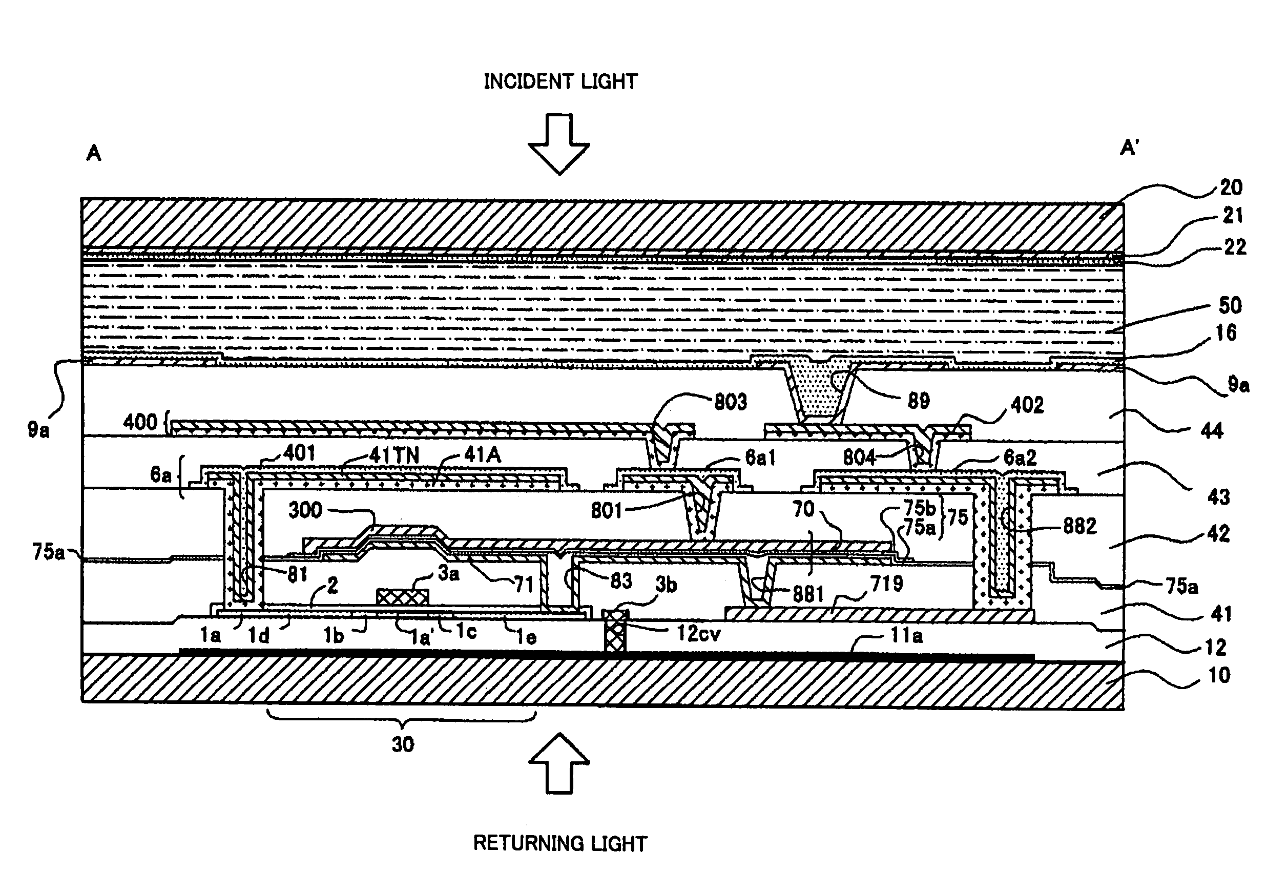
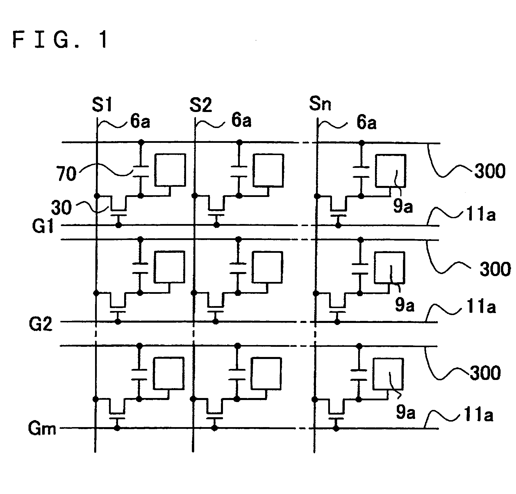
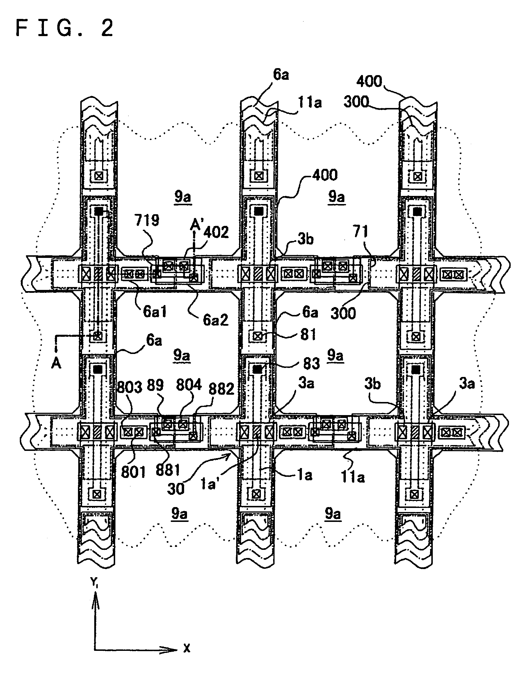
[0064]A configuration of each pixel portion of an electro-optical device according to an exemplary embodiment of the present invention is described with reference to FIGS. 1 to 4. FIG. 1 is a schematic showing an equivalent circuit including various elements and wiring lines for pixels arranged in a matrix, which constitute an image display region of the electro-optical device. FIG. 2 is a plan view showing a plurality of the pixels, adjacent to each other, placed on a TFT array substrate having data lines, scanning lines, and pixel electrodes thereon. FIG. 3 is a plan view showing only a principal portion of FIG. 2. In particular, FIG. 3 is a plan view showing the arrangement of the data lines, shield...


PUM


Abstract

An electro-optical device includes above a substrate: data lines extending in a first direction; scanning lines extending in a second direction in such a manner that the scanning lines and data lines cross each other; pixel electrodes and thin-film transistors each placed in corresponding regions corresponding to intersections of the scanning lines and data lines; storage capacitors disposed below the data lines and each electrically connected to the corresponding thin-film transistors and pixel electrodes; a capacitor line disposed above the data lines; first junction electrodes, formed using the same film used to form the data lines, each electrically connecting the corresponding pixel potential capacitor electrodes of the storage capacitors and pixel electrodes; and second junction electrodes, formed using the same film as that to form the data lines, each electrically connecting the corresponding constant potential capacitor electrodes of the storage capacitors and the capacitor line. The data lines, first junction electrodes, and second junction electrodes each including a nitride film.

Description

BACKGROUND OF THE INVENTION[0001]1. Field of Invention[0002]The present invention relates to an electro-optical device, such as a liquid crystal device and an electronic apparatus including such an electro-optical device. The present invention also relates to an electroluminescent (EL) device, a device including an electron-emitting element, and an electrophoretic device, such as an electronic paper sheet, wherein the electron-emitting element-including device includes field emission displays and surface-conduction electron-emitter displays.[0003]2. Description of Related Art[0004]Electro-optical devices, such as liquid crystal devices, each including the following components have been known: a pair of substrates and electro-optical materials, such as liquid crystals, placed therebetween. In such electro-optical devices, an image can be displayed by allowing light to pass through the substrates and electro-optical materials. The display of an image can be achieved as follows: the tr...

Claims


Application Information

Patent Timeline
IPC IPC(8): H01L29/04H01L31/036G02F1/1333G02F1/1343G02F1/136G02F1/1362G02F1/1368G09F9/30H01L27/32H01L51/50H05B33/10
CPCG02F1/136213G02F1/136209H01L27/3297G02F1/136227H10K59/1315H10K59/131G02F1/136
Inventor KURASHINA, HISAKITAKAHARA, KENICHIKAWATA, HIDENORI
Owner 138 EAST LCD ADVANCEMENTS LTD
Why Eureka
Try Eureka