Bypass filter, multi-band antenna switch circuit, and layered module composite part and communication device using them

a multi-band antenna switch circuit and composite part technology, applied in the field of wireless communication systems, can solve the problems of unsuitably large volume and weight of mobile communications devices, unsuitable high-frequency parts, and sometimes disconnected mobile phones

Inactive Publication Date: 2006-06-06
MURATA MFG CO LTD
View PDF18 Cites 203 Cited by
  • Summary
  • Abstract
  • Description
  • Claims
  • Application Information

AI Technical Summary

Benefits of technology

[0024]Accordingly, an object of the present invention is to solve a problem (1) concerning the breakdown of high-frequency parts by electrostatic surge, a problem (2) concerning harmonic generation, and a problem (3) concerning miniaturization, power-saving and harmonic generation as described above, thereby providing an electrostatic-surge-removing highpass filter, a multiband antenna switch circuit with suppressed harmonic generation, particularly a multiband antenna switch circuit free from the problem of harmonic generation caused by using an FET switch for miniaturization and power saving, and a laminate module and communications device comprising such part.

Problems solved by technology

According to recent rapid expansion of mobile phones, however, a frequency band allocated to each system cannot allow all users to use their mobile phones in major cities in advanced countries, resulting in difficulty in connection and thus causing such a problem that mobile phones are sometimes disconnected during communication.
Accordingly, such mobile communications devices are not only expensive but also have unsuitably large volume and weight.
(1) Breakdown of High-Frequency Parts by Electrostatic Surge
Particularly in the case of mobile phones, the above high-frequency parts are subjected to breakdown when electrostatic surge from human bodies is input into antennas.
In addition, though an antenna switch module per se is not subjected to breakdown, circuits connected downstream of the antenna switch module, such as power amplifiers and low-noise amplifiers, etc. connected to transmission terminals and receiving terminals, respectively, of the antenna switch module are likely subjected to breakdown.
When an inductor of 5 nH or less is connected to an antenna top, however, it is difficult to secure matching in a wide band from 900 MHz to 1.8 GHz.
Attenuation near 300 MHz is actually as small as 5 dB or less in this circuit, insufficient for the removal of electrostatic surge.
However, the insertion of an LC filter comprising an inductor L1 and a capacitor C1 in each of the antenna terminal, the transmission terminal and the receiving terminal not only prevents the miniaturization and cost reduction of a high-frequency switch, but also causes the deterioration of insertion loss.
Attenuation near 300 MHz is actually as small as about 5 dB in this circuit, insufficient for the removal of electrostatic surge.
Though it may be considered to use varistor diodes and Zener diodes as electrostatic-surge-removing parts, it necessitates a large capacitance between the terminals, inevitably resulting in the deterioration of insertion loss when used in signal lines.
Accordingly, the varistor diode and the Zener diode cannot be used to remove electrostatic surge in a high-frequency circuit comprising high-frequency switches.
The circuit shown in FIG. 31 has a problem that harmonic strain is generated by a W-CDMA transmission signal passing through the second high-frequency switch SW2.
On the other hand, the operation point of the diode is around V=0 in an OFF state, so that the diode unlinearly responds to voltage change by high-frequency signals, resulting in large harmonic generation.
This means that a signal that should not be emitted from an antenna of a mobile phone is emitted, a problem unavoidable in the conventional art.
However, because the switch circuit SW is connected to the diplexer Dip1 on a transmitting side in an EGSM transmission mode, there is a problem that a DCS band signal supplied from the DCS transmission terminal (Tx) also passes.
There is basically a problem that a GaAs switch is more likely to generate harmonic strain than a circuit comprising pin diodes.
However, it is difficult at present to obtain GaAs switches with such small harmonic generation.
In the case of a circuit comprising a GaAs switch directly switching transmitting and receiving signals of plural frequencies without using a diplexer, the GaAs switch is more vulnerable to breakdown by electrostatic surge than a pin diode.
However, when the inductor of 5 nH or less is connected to an antenna top, it is difficult to obtain matching in a wide band from 900 MHz to 1.8 GHz.
Because of this, too, the conventional electrostatic-surge-removing circuit cannot be used on an antenna top.

Method used


Image

  • Bypass filter, multi-band antenna switch circuit, and layered module composite part and communication device using them
  • Bypass filter, multi-band antenna switch circuit, and layered module composite part and communication device using them
  • Bypass filter, multi-band antenna switch circuit, and layered module composite part and communication device using them

Examples


example 1

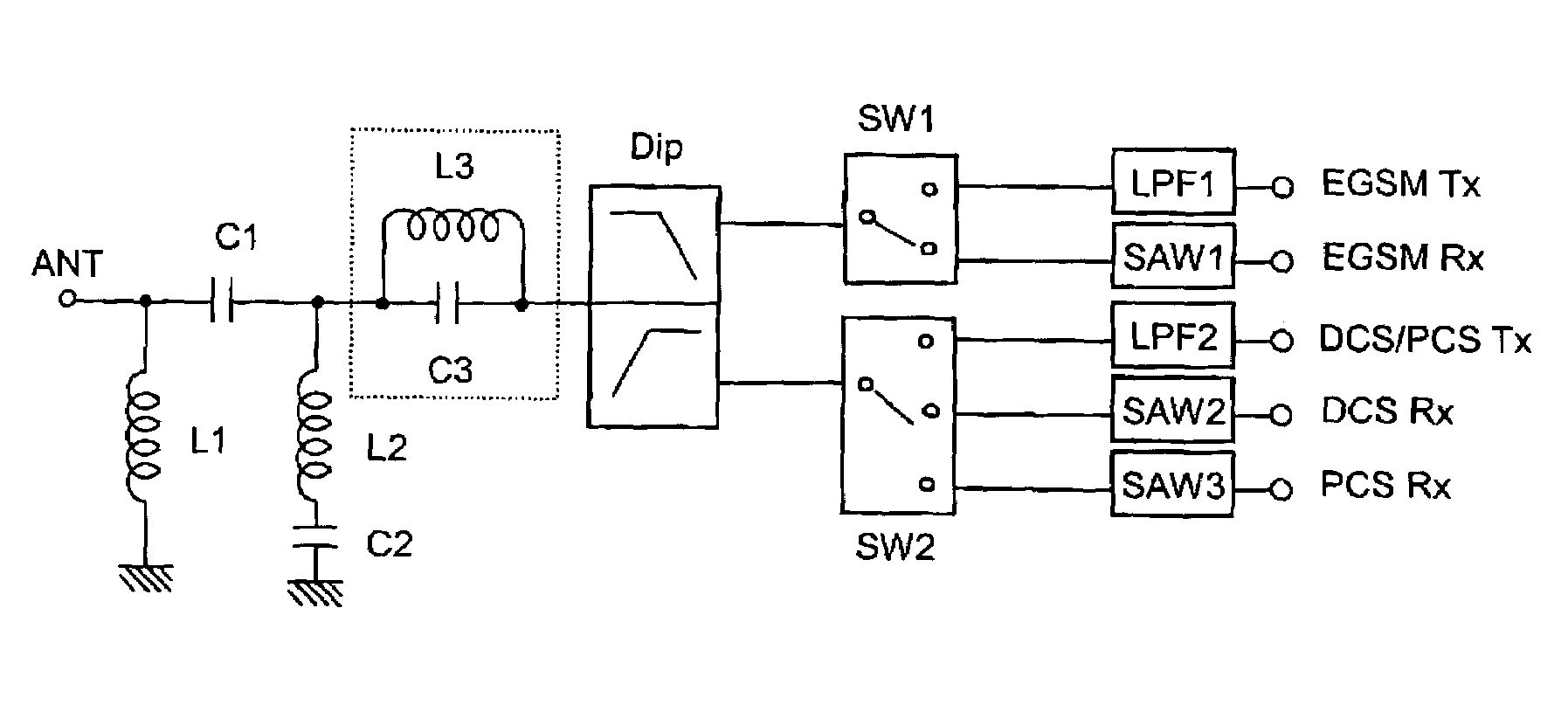
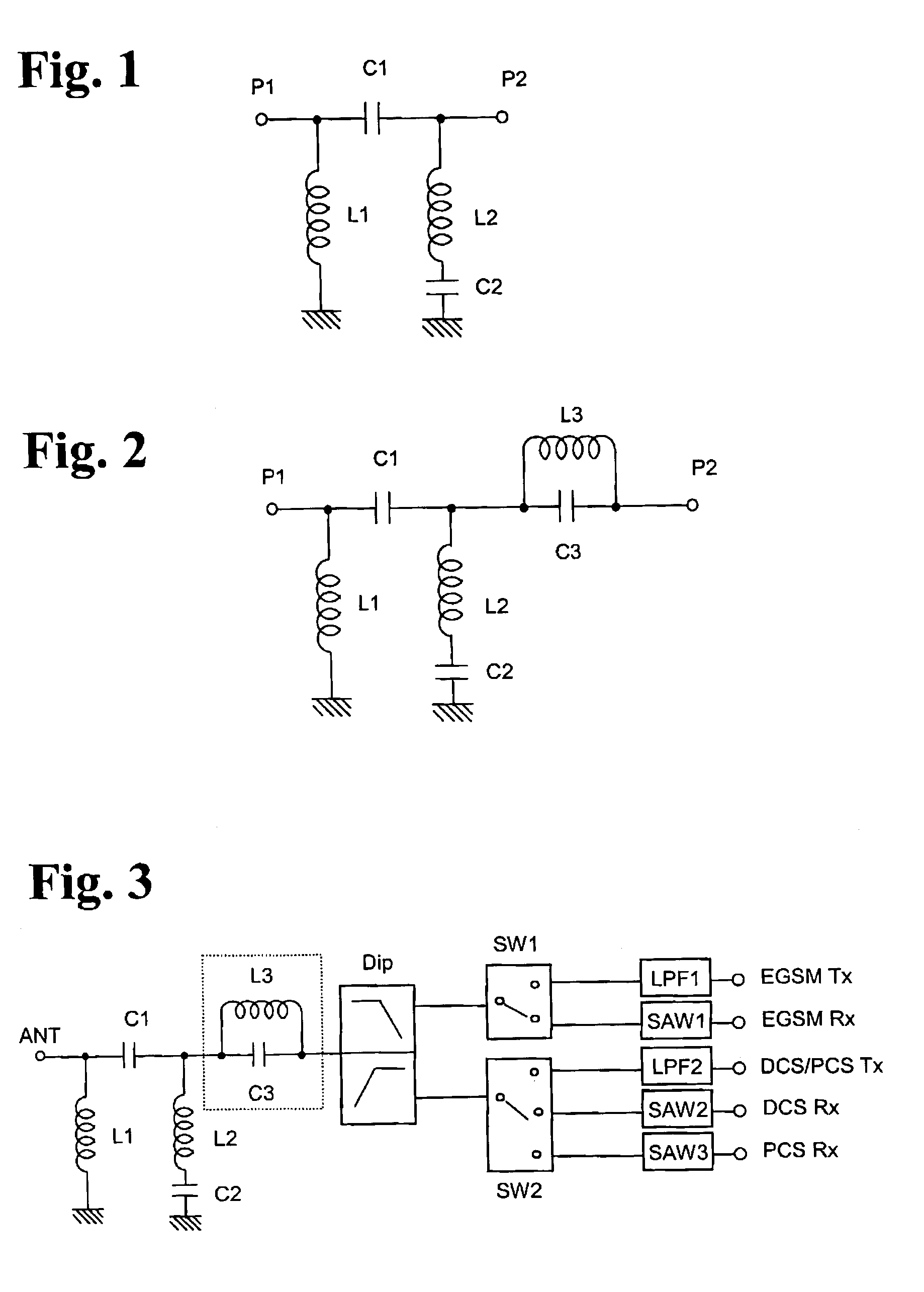
[0088]FIG. 3 is a block diagram showing one example of a tripleband antenna switch circuit comprising the electrostatic-surge-removing highpass filter of the present invention. In this Example, the diplexer Dip causes branching to an EGSM-band signal (880 to 960 MHz) and a DCS / PCS-band signal (DCS: 1710 to 1880 MHz, PCS: 1850 to 1990 MHz). The switch circuit SW1 switches the transmitting and receiving of EGSM, and the switch circuit SW2 switches DCS / PCS transmission, DCS receiving and PCS receiving. The lowpass filter LPF1 attenuates an n-th harmonic strain contained in a transmission signal sent from the EGSM TX terminal, and the lowpass filter LPF2 attenuates an n-th harmonic strain contained in a transmission signal sent from the DCS / PCS TX terminal. The SAW filters SAW1, SAW2, SAW3 remove noises outside the receiving band from each receiving signal of EGSM, DCS and PCS.

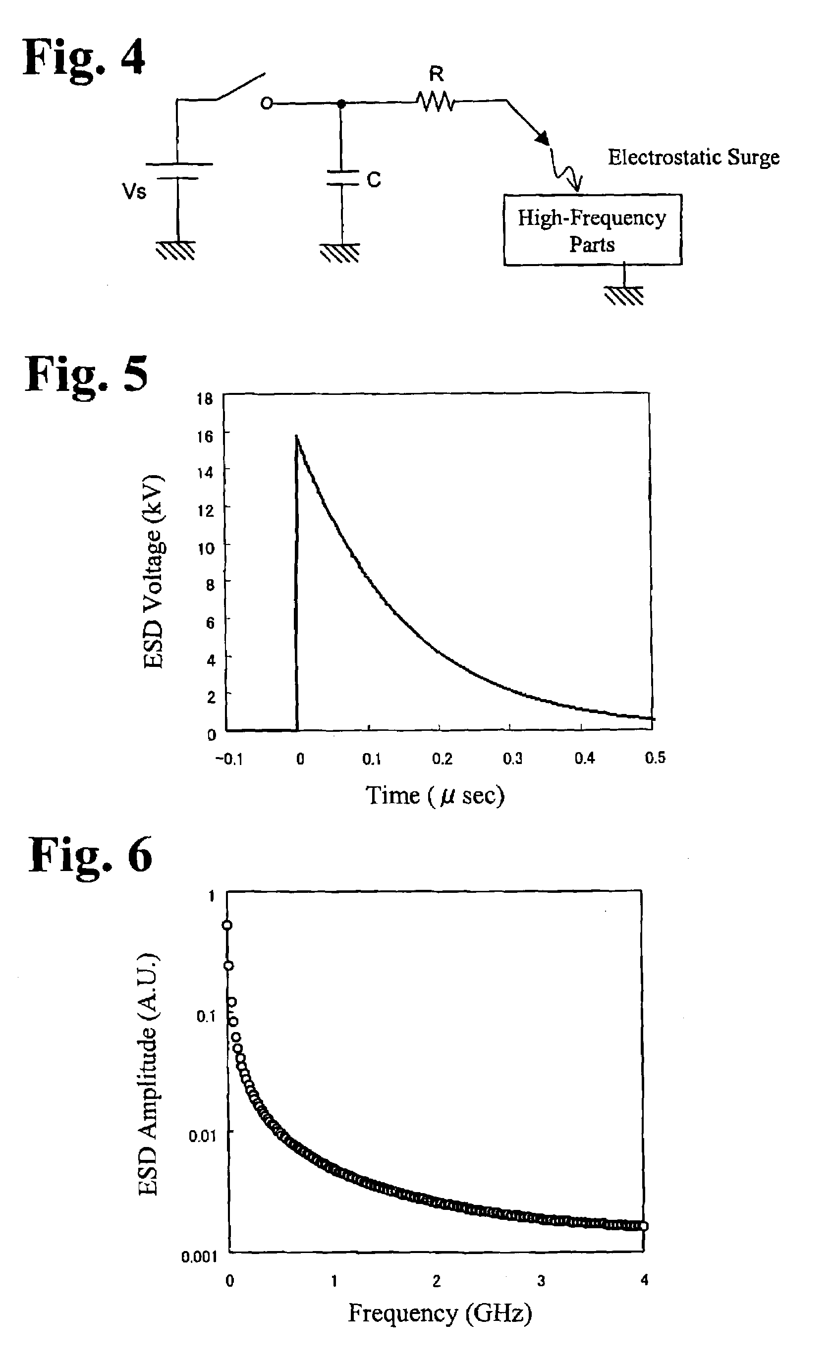
[0089]The electrostatic-surge-removing circuit disposed between the antenna terminal ANT and the diplexer Dip c...

example 2

[0095]FIG. 9 is a block diagram showing a tripleband antenna switch circuit adapted for EGSM, DCS and W-CDMA according to one embodiment of the present invention. Branched by the diplexer Dip are signals from the antenna in a band of 880 to 960 MHz for EGSM (transmission frequency: 880 to 915 MHz, receiving frequency: 925 to 960 MHz), and in a band of 1710 to 2170 MHz for DCS (transmission frequency: 1710 to 1785 MHz, receiving frequency: 1805 to 1880 MHz) and W-CDMA (transmission frequency: 1920 to 1980 MHz, receiving frequency: 2110 to 2170 MHz).

[0096]The switch circuit SW1 switches EGSM signals branched by the diplexer Dip to the transmission terminal EGSM Tx and the receiving terminal EGSM Rx. The switch circuit SW2 switches DCS or W-CDMA signals branched by the diplexer Dip to the transmission terminal DCS Tx, the receiving terminal DCS Rx and the transmitting / receiving terminal W-CDMA. To suppress n-th harmonic strain included in transmission signals sent from the power amplif...

example 3

[0115]FIG. 11 is a block diagram showing an antenna switch circuit adapted for EGSM, DCS and W-CDMA. The circuit of this Example is the circuit shown in FIG. 9, in which a first notch filter NF1 is disposed between the diplexer Dip and the first switch circuit SW1. The notch filter NF1 may comprise a parallel resonance circuit and / or a serial resonance circuit shown in FIGS. 14(a) and 14(b), respectively. In this case, the resonance frequency is preferably set to be two or three times the transmission frequency of EGSM. Because the notch filter NF1 removes harmonic strain generated at the first high-frequency switch SW1 in this Example, harmonics generated by the antenna is further suppressed.


PUM


Abstract

A multi-band antenna switch circuit including a diplexer connected to an antenna terminal for demultiplexing signals of different passing bands, a first and a second switch circuit for switching a high frequency signal and a low frequency signal demultiplexed by the diplexer to a plurality of transmission / reception terminals, a first and a second low pass filter connected to a transmission path between the diplexer and the transmission terminal or between the first and the second switch circuit and the transmission terminal, and a notch filter provided between the diplexer and the first switch circuit or between the diplexer and the second switch circuit. The multi-band antenna switch circuit includes a high pass filter having an input terminal and an output terminal and provided at least between die diplexer and the antenna terminal and including a first inductor connected between the input terminal and the ground, a first capacitor connected between the input terminal and the output terminal, a second inductor connected to the output terminal, and a second capacitor connected between the second inductor and the ground.

Description

CROSS REFERENCE TO RELATED APPLICATIONS[0001]This application is a national phase application based on PCT / JP02 / 08215, filed Aug. 12, 2002, the content of which is incorporated herein by reference, and claims the priority of Japanese Patent Application No. 2001-244343, filed Aug. 10, 2001, Japanese Patent Application No. 2001-264843, filed Aug. 31, 2001, and Japanese Patent Application No. 2002-073910, filed Mar. 18, 2002.FIELD OF THE INVENTION[0002]The present invention relates to a wireless communications system connected to a common antenna for transmitting and receiving two or more signals having different frequencies, particularly to a multiband antenna switch circuit, and a composite laminate multiband antenna switch module and a communications device both comprising the multiband antenna switch circuit.BACKGROUND OF THE INVENTION[0003]There are various systems for mobile phones, for instance, EGSM (extended global system for mobile communications) and DCS (digital cellular sy...

Claims


Application Information

Patent Timeline
Patent Type & Authority Patents(United States)
IPC IPC(8): H01P1/10H03H7/46H03H7/01H03H7/075H04B1/40H04B1/44H04B1/48H04B1/52
CPCH03H7/0115H03H7/0153H03H7/1766H03H7/1783H03H7/465H04B1/52H04B1/0057H04B1/006H04B1/406H04B1/48H03H7/1758H04B1/44H03H2001/0085
Inventor FUKAMACHI, KEISUKEKEMMOCHI, SHIGERUWATANABE, MITSUHIROTAKETA, TSUYOSHITAI, HIROYUKIYOKOUCHI, SATORU
Owner MURATA MFG CO LTD
Why Eureka
Try Eureka