Optical scanning apparatus, image forming apparatus, and methods of performing optical scanning using optical scanning apparatus and image forming apparatus
a technology of optical scanning which is applied in the field of optical scanning apparatus and image forming apparatus, can solve the problems of field angle, focus error, irregular density of image,
- Summary
- Abstract
- Description
- Claims
- Application Information
AI Technical Summary
Benefits of technology
Problems solved by technology
Method used
Image

Examples
second embodiment
[Second Embodiment]
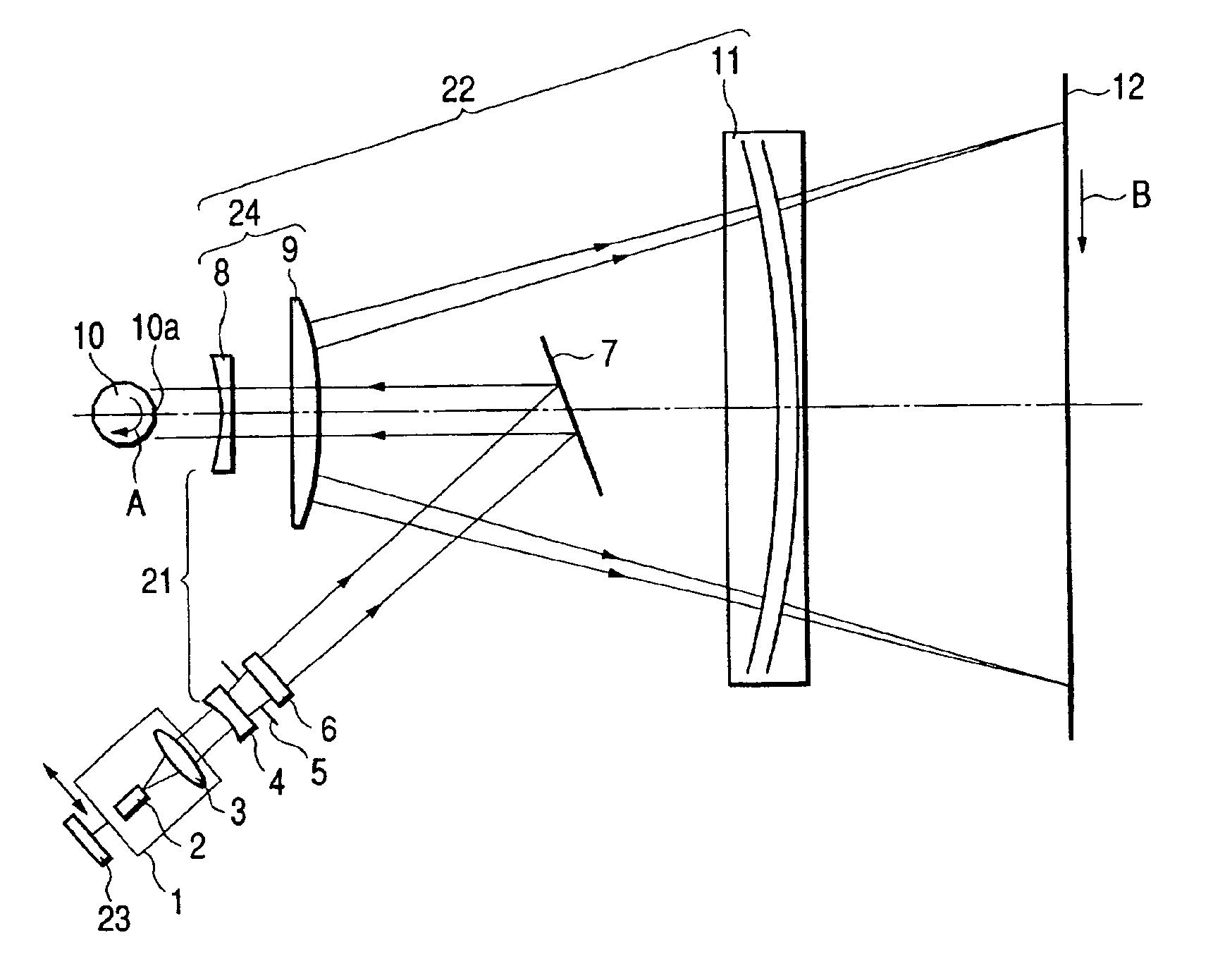
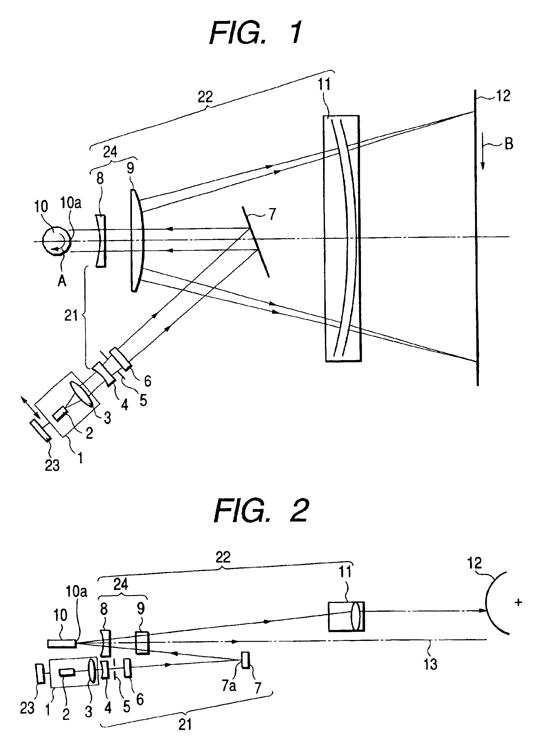
[0057]FIG. 4 is a sectional view (main scanning sectional view) of the main part of the second embodiment of the present invention in the main scanning direction. FIG. 5 is a sectional view (sub-scanning sectional view) of the main part in FIG. 4 in the sub-scanning direction. The same reference numerals as in FIGS. 1 and 2 denote the same parts in FIGS. 4 and 5.
[0058]This embodiment differs from the first embodiment describe above in that a light beam emerging from an incident optical system 21 is obliquely incident on a deflecting surface 10a of an optical deflector 10 within a main scanning cross-section, and the incident optical system 21 is placed in a reflecting / deflecting (deflection scanning) plane based on the optical deflector 10. Other arrangements and optical functions are substantially the same as those in the first embodiment, and hence similar effects are obtained.
[0059]Since the optical axis of the incident optical system 21 in this embodiment is l...
third embodiment
[Third Embodiment]
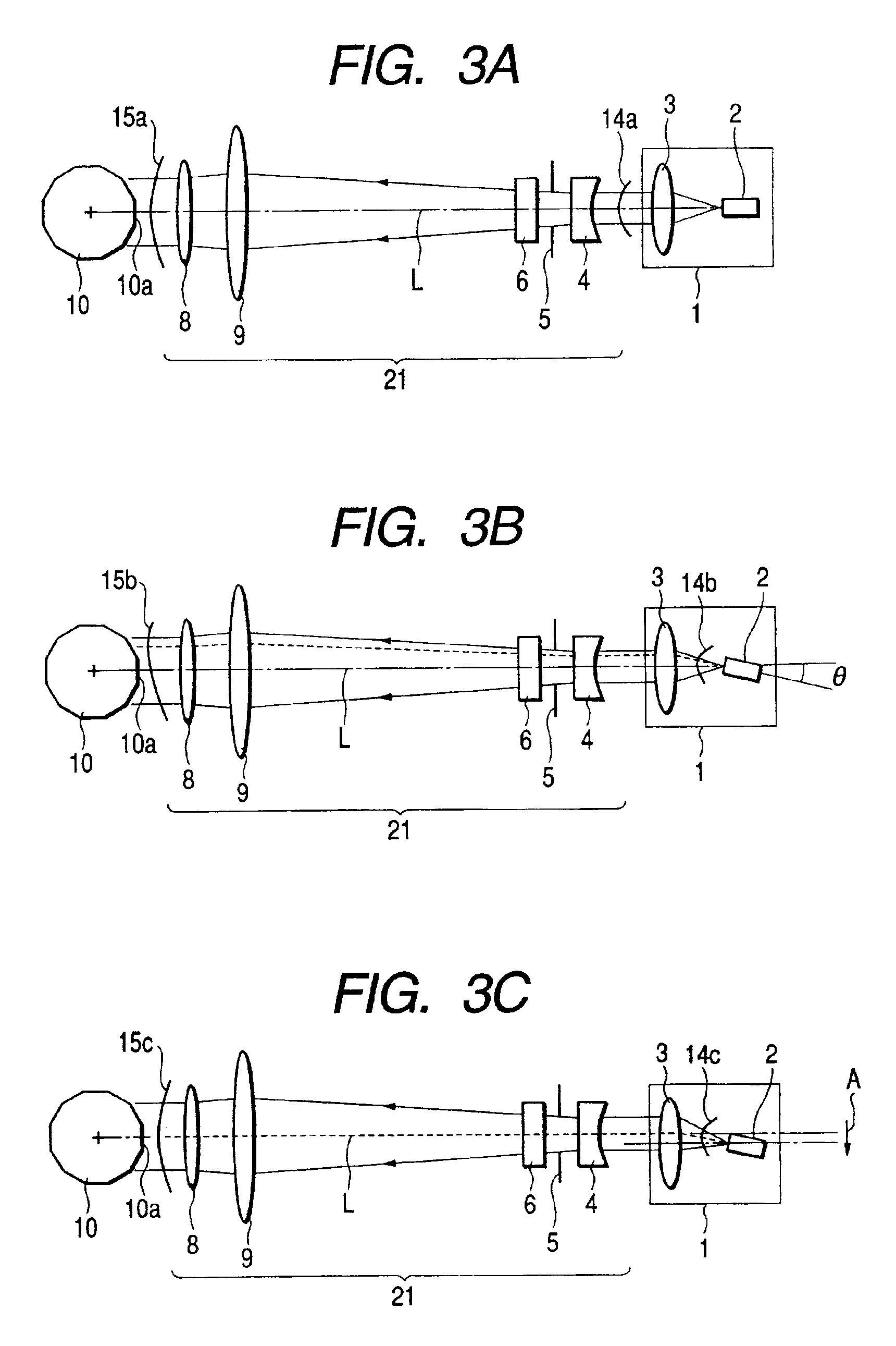
[0062]The third embodiment of the present invention will be described next.
[0063]This embodiment differs from the first embodiment described above in that a laser unit is shifted by a shift adjusting means in the main scanning direction (vertical direction) with respect to the optical axis of an incident optical system such that the ratio of the intensities of two light beams obtained by splitting a light beam passing through a stop plate in two at the stop center in the main scanning direction becomes 10% or less. Other arrangements and optical functions are substantially the same as those in the first embodiment, and hence similar effects are obtained.
[0064]To reduce the asymmetry of an illuminance distribution on a scanned surface due to variations in components, assembly errors, and the like, the ratio of the light intensities of light beams passing through the stop plate in the main scanning direction must be set to 10% or less. In this embodiment, therefore, ...
fourth embodiment
[Fourth Embodiment]
[0065]The fourth embodiment of the present invention will be described next.
[0066]This embodiment differs from the first embodiment described above in that a semiconductor laser and collimator lens are integrated into a chip such that the tilt angle of the chip in the main scanning direction of the semiconductor laser is set to ±2.5° or less with respect to the optical axis of the collimator lens. Other arrangements and optical functions are substantially the same as those in the first embodiment, and hence similar effects are obtained.
[0067]The reason why the tilt angle of the chip in the main scanning direction of the semiconductor laser is set to ±2.5° or less with respect to the optical axis of the collimator lens will be described below.
[0068]Letting f be the focal length of the collimator lens and θ be the tilt angle of the chip in the main scanning direction, a shift amount L of the laser unit which is required to obtain a symmetrical intensity distribution...
PUM
 Abstract
Description
Claims
Application Information
 - Generate Ideas
- Intellectual Property
- Life Sciences
- Materials
- Tech Scout
- Unparalleled Data Quality
- Higher Quality Content
- 60% Fewer Hallucinations
Browse by: Latest US Patents, China's latest patents, Technical Efficacy Thesaurus, Application Domain, Technology Topic, Popular Technical Reports.
© 2025 PatSnap. All rights reserved.Legal|Privacy policy|Modern Slavery Act Transparency Statement|Sitemap|About US| Contact US: help@patsnap.com