Optical module with lens integral holder fabrication method

a technology of optical modules and integral holders, applied in the field of electronic components packaging, can solve the problems of large image sensor assembly and relatively large housing, and achieve the effects of minimizing the overall width enhancing the environmental protection and reliability of the optical module, and minimizing the cost associated

Inactive Publication Date: 2006-06-13
AMKOR TECH SINGAPORE HLDG PTE LTD
View PDF87 Cites 46 Cited by
  • Summary
  • Abstract
  • Description
  • Claims
  • Application Information

AI Technical Summary

Benefits of technology

[0019]By forming either the mounting surface or the joint surface as a locking feature, the environmental protection as well as reliability of the optical module is enhanced while at the same time the overall width of the optical module is minimized.
[0020]To minimize the cost associated with fabricating the optical module, in one embodiment, a plurality of optical modules are fabricated simultaneously in an ...

Problems solved by technology

However, this housing was relatively bulky and, as ...

Method used


Image

  • Optical module with lens integral holder fabrication method
  • Optical module with lens integral holder fabrication method
  • Optical module with lens integral holder fabrication method

Examples


Embodiment Construction

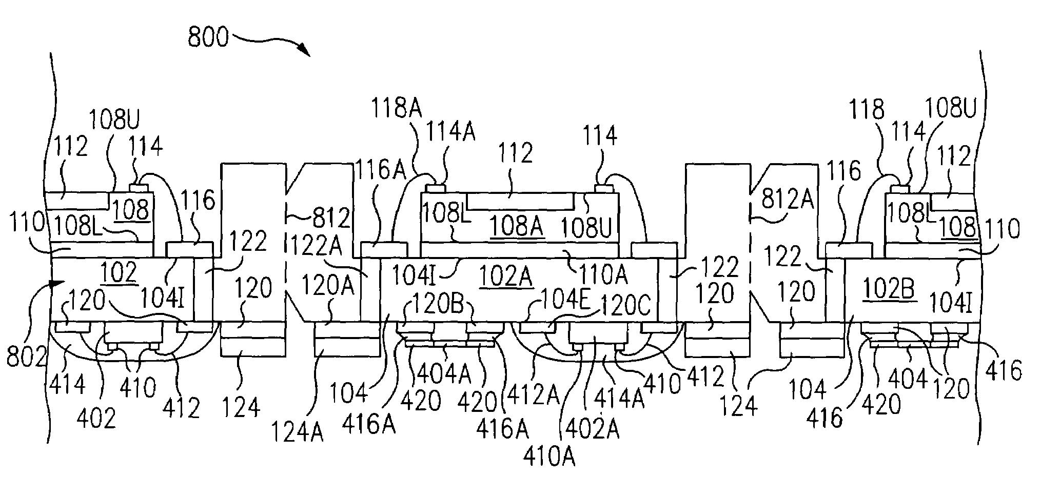
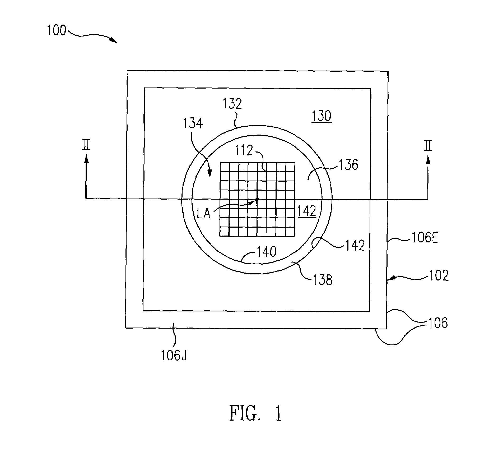
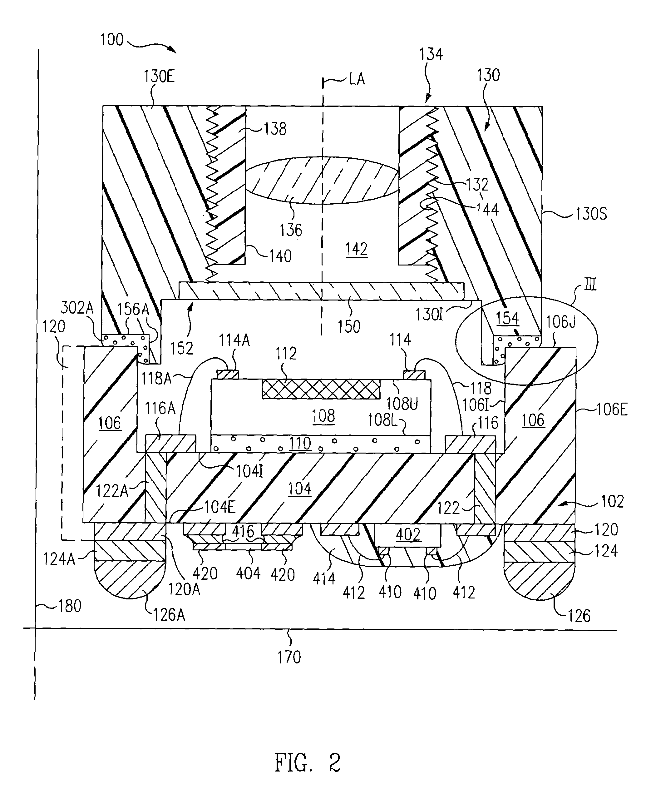
[0034]In accordance with the present invention, an optical module 100 (FIG. 2) includes a substrate 102 having a base 104 and a sidewall 106. Optical module 100 further includes an image sensor 108 mounted to base 104 and a lens housing 130 mounted to sidewall 106.

[0035]Sidewall 106 includes a joint surface 106J and lens housing 130 includes a mounting surface 156A. Mounting surface 156A of lens housing 130 is bonded to joint surface 106J of substrate 102 thus mounting lens housing 130 to sidewall 106.

[0036]To minimize the overall width of optical module 100, in one embodiment (FIG. 3B), mounting surface 156A of lens housing 130 is formed with a locking feature. The locking feature includes a horizontal surface 310 parallel to joint surface 106J of substrate 102 and a vertical surface 312 perpendicular to joint surface 106J and extending downwards from horizontal surface 310. Horizontal surface 310 is bonded to joint surface 106J and vertical surface 312 is bonded to an interior sur...


PUM

PropertyMeasurementUnit
Adhesivityaaaaaaaaaa
Areaaaaaaaaaaa

Abstract

A method of forming an optical module includes mounting an image sensor to a base of a substrate and bonding a lens housing to a sidewall of the substrate. A mounting surface of the lens housing includes a locking feature having a horizontal surface and a vertical surface. The sidewall of the substrate includes a joint surface. To bond the lens housing to the sidewall of the substrate, a bond is formed between the horizontal surface of the locking feature of the lens housing and the joint surface of the sidewall. Further, a bond is formed between the vertical surface of the locking feature of the lens housing and an interior surface of the sidewall.

Description

BACKGROUND OF THE INVENTION[0001]1. Field of the Invention[0002]The present invention relates generally to the packaging of electronic components. More particularly, the present invention relates to a method for fabricating an optical module.[0003]2. Description of the Related Art[0004]Image sensors are well known to those of skill in the art. An image sensor included an active area, which was responsive to electromagnetic radiation. The image sensor was used to fabricate an image sensor assembly.[0005]In one prior art image sensor assembly, the image sensor was located within a housing, which supported a window. Radiation passed through the window and struck the active area of the image sensor, which responded to the radiation.[0006]To form the image sensor assembly, the image sensor was mounted to a printed circuit mother board. After the image sensor was mounted, a housing was mounted around the image sensor and to the printed circuit mother board. This housing provided a seal ar...

Claims


Application Information

Patent Timeline
IPC IPC(8): H05K3/20
CPCG02B7/02H01L24/97H01L27/14618H01L27/14625H01L27/14632H01L27/14685H01L27/14687H01L31/0203H01L31/0232H04N5/2253H04N5/2254H04N5/2257H01L2224/32225H01L2224/48091H01L2224/48227H01L2224/73265H01L2224/97H01L2924/01013H01L2924/01057H01L2924/01082H01L2924/15311H01L2924/19041H01L2924/01023H01L2924/01033H01L2924/12041H01L2924/15153Y10T29/4913Y10T29/49787Y10T29/49128Y10T29/49146H01L2924/00014H01L2224/83H01L2224/85H01L2924/00H01L2924/00012H01L24/73H01L2924/14H01L31/02325H04N23/54H04N23/57H04N23/55
Inventor WEBSTER, STEVENGLENN, THOMAS P.HOLLAWAY, ROY DALE
Owner AMKOR TECH SINGAPORE HLDG PTE LTD
Why Eureka
Try Eureka