Chip package structure and manufacturing method thereof

a technology of chip package and manufacturing method, which is applied in the direction of semiconductor devices, semiconductor/solid-state device details, electrical equipment, etc., can solve the problems of increasing cost, complexity, uncertainty of fabrication process, and complexity of electrical product design, and achieves higher heat dissipation efficiency and integration. , the effect of high efficiency

Active Publication Date: 2006-06-13
ADVANCED SEMICON ENG INC
View PDF2 Cites 143 Cited by
  • Summary
  • Abstract
  • Description
  • Claims
  • Application Information

AI Technical Summary

Benefits of technology

[0010]The present invention provides a chip package structure and the manufacturing method thereof, which affords higher heat dissipation efficiency and is suitable to fabricate the stack type package structure with a higher integration.
[0014]Because the heat sink is disposed over the chip and a mold compound is formed between the chip and the heat sink, heat generated by the chip can be dissipated by the heat sink via the mold compound. In this invention, the connecting portions of the heat sink are disposed around a periphery of the body and connected to the leads. By using a specially designed heat sink, the chip package structure can afford better heat dissipation and be suitable to form stack type package structures.

Problems solved by technology

Following the quick progress in the fabrication of integrated circuits, the design of the electrical products becomes more complex and high-speed and multi-function chips are developed.
Therefore, the costs, the complexity and the uncertainty of the fabrication processes are increased.

Method used


Image

  • Chip package structure and manufacturing method thereof
  • Chip package structure and manufacturing method thereof
  • Chip package structure and manufacturing method thereof

Examples


Embodiment Construction

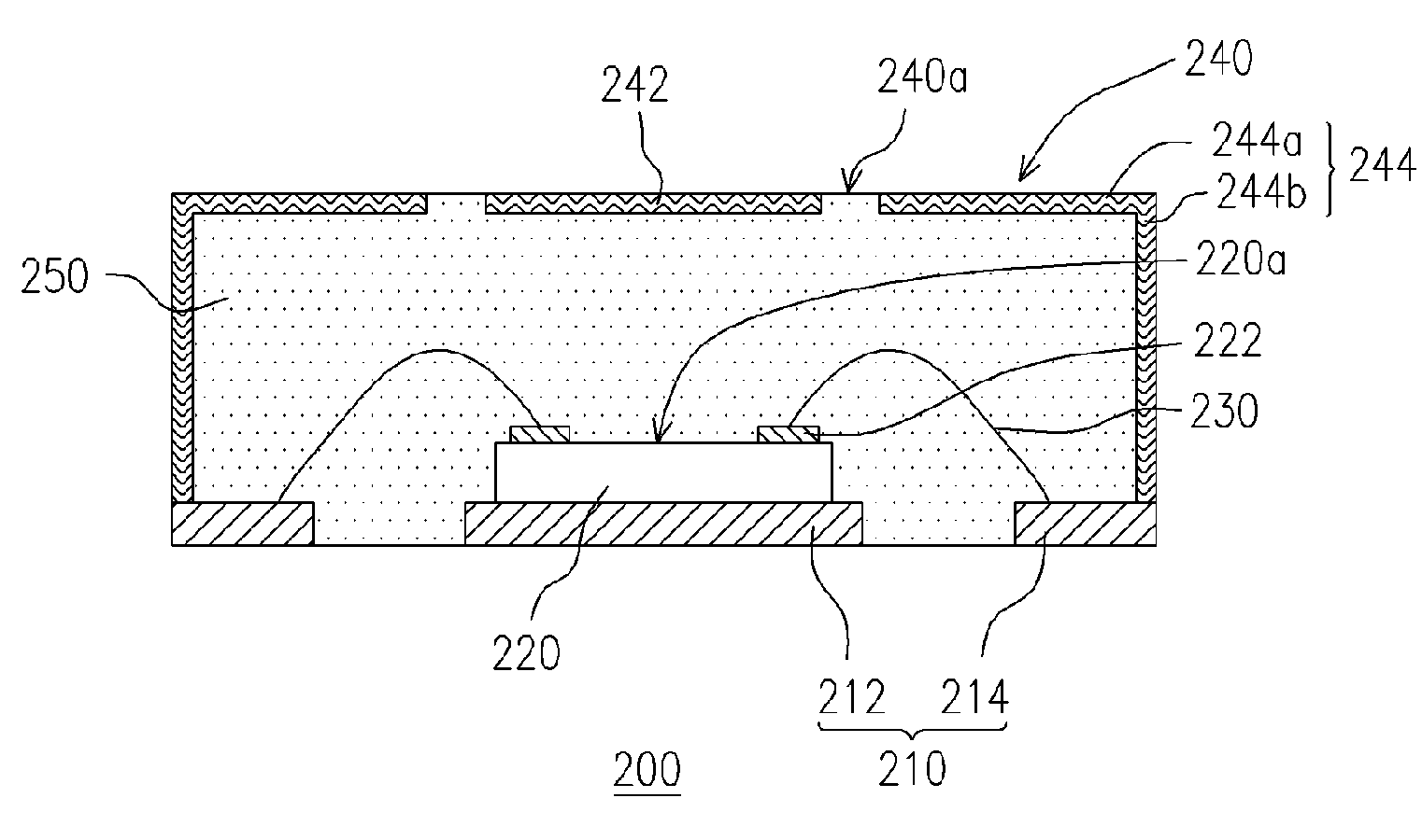
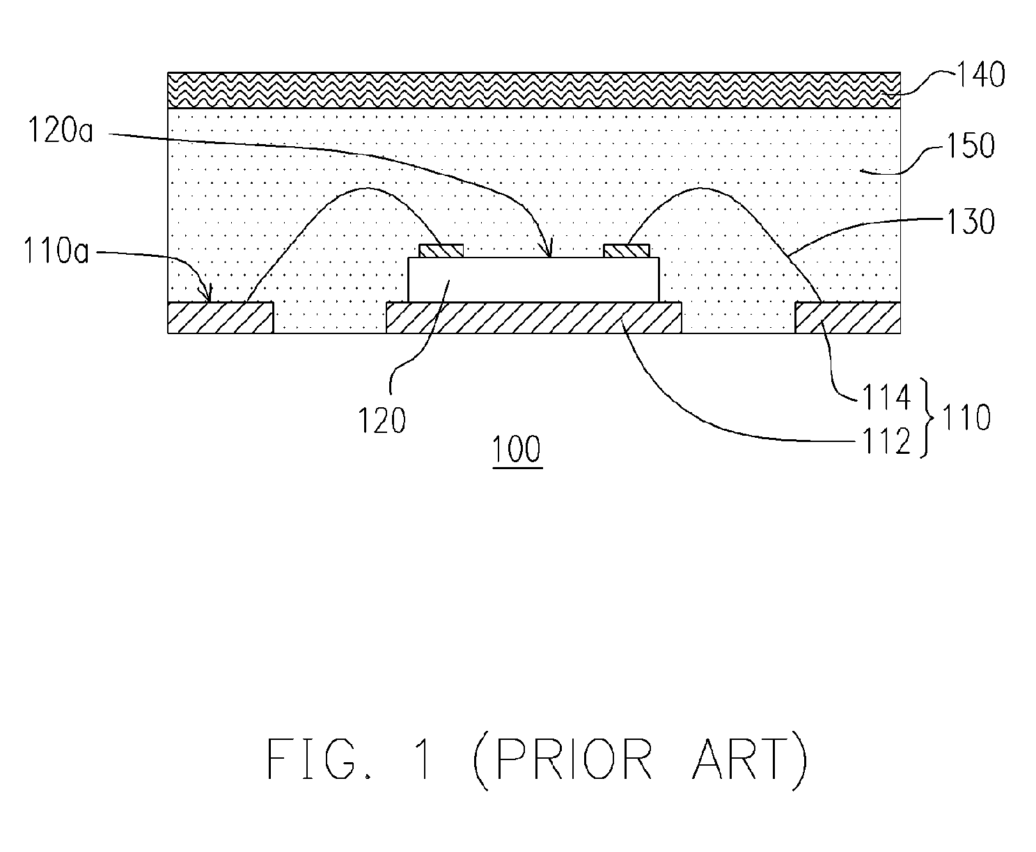
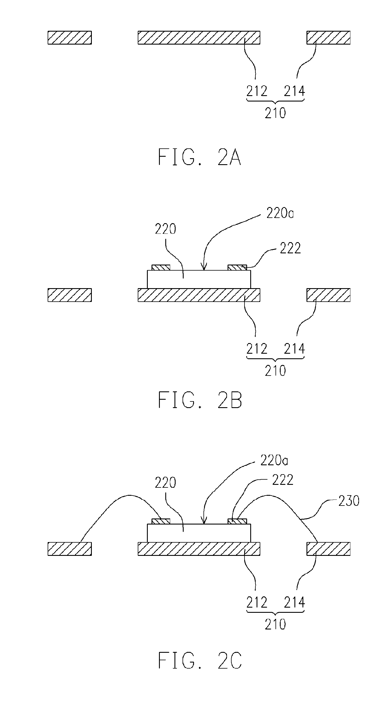
[0022]FIGS. 2A–2F are display cross-sectional views showing the manufacturing process steps of a QFN package structure according to the first preferred embodiment of the present invention. Referring to FIG. 2A, a leadframe 210 used as a carrier is provided. The leadframe 210 includes a die pad 212 and a plurality of leads 214. As shown in FIG. 2B, a chip 220 is disposed on the die pad 212. The chip 220 has an active surface 220a and a plurality of bonding pads 222 on the active surface 220a. Referring to FIG. 2C, each of the leads 214 is connected to one bonding pad 222 through a plurality of wires 230 by, for example, wire bonding.

[0023]Referring to FIG. 2D, a heat sink (or heat dissipation plate) 240 is provided. The heat sink 240 is made of a conductive material and has a body 242, a plurality of connecting portions 244 and a plurality of protrusions 246. The heat sink may be in a spider shape from the top view, for example. The connecting portions 244 are disposed around the edg...


PUM


Abstract

The present invention provides a chip package structure and the manufacturing method thereof, which affords higher heat dissipation efficiency and is suitable to fabricate the stack type package structure with a higher integration. The chip package structure comprises a carrier, at least a chip, a heat sink and a mold compound. The chip is disposed on the carrier, while the bonding pads of the chip are electrically connected to the leads of the carrier. The heat sink is disposed over the chip and includes at least a body and a plurality of connecting portions. The connecting portions are disposed around a periphery of the body and are electrically connected to the leads. By using a specially designed heat sink, the chip package structure can afford better heat dissipation and be suitable to form stack type package structures.

Description

CROSS-REFERENCE TO RELATED APPLICATION[0001]This application claims the priority benefit of Taiwan application Ser. no. 92132104, filed on Nov. 17, 2003.BACKGROUND OF THE INVENTION[0002]1. Field of Invention[0003]The present invention relates to a package structure and the manufacturing method thereof. More particularly, the present invention relates to a stacked chip package structure and the manufacturing method thereof.[0004]2. Description of Related Art[0005]Following the quick progress in the fabrication of integrated circuits, the design of the electrical products becomes more complex and high-speed and multi-function chips are developed. As the integration of ICs keeps increasing and the layout of the high-speed semiconductor devices becomes dense, more heat is generated by the semiconductor device per unit area in a certain period. Thus, it is important for the design of semiconductor devices to consider the heat dissipation issue, in order to prevent damages to the electron...

Claims


Application Information

Patent Timeline
Patent Type & Authority Patents(United States)
IPC IPC(8): H01L23/495H01L21/48H01L23/31H01L23/34H01L23/36H01L23/433H01L25/10
CPCH01L23/3107H01L23/4334H01L23/49517H01L24/48H01L25/105H01L2224/05571H01L2224/05573H01L2224/16H01L2224/16245H01L2224/48091H01L2224/48247H01L2225/1029H01L2924/00014H01L2924/14H01L2924/181H01L2924/1815H01L2924/00H01L2224/05599H01L2924/00012H01L2224/45099H01L2224/45015H01L2924/207
Inventor WENG, GWO-LIANGLEE, SHIH-CHANGLEE, CHENG-YIN
Owner ADVANCED SEMICON ENG INC
Why Eureka
Try Eureka