Light emitting device and electronic device

a technology of which is applied in the field of organic light emitting devices and electronic devices, can solve the problems of reducing contrast or disturbing display images, and limit the reduction of off current, so as to prevent disturbance of displayed images and suppress contrast.

Inactive Publication Date: 2006-06-13
SEMICON ENERGY LAB CO LTD
View PDF25 Cites 215 Cited by
  • Summary
  • Abstract
  • Description
  • Claims
  • Application Information

AI Technical Summary

Benefits of technology

[0030]According to the above structure, even if the off current flows into the driver TFT, light emission of the

Problems solved by technology

This becomes a cause of reduced contrast or disturbed display image.
However, in ei

Method used


Image

  • Light emitting device and electronic device
  • Light emitting device and electronic device
  • Light emitting device and electronic device

Examples


embodiment 1

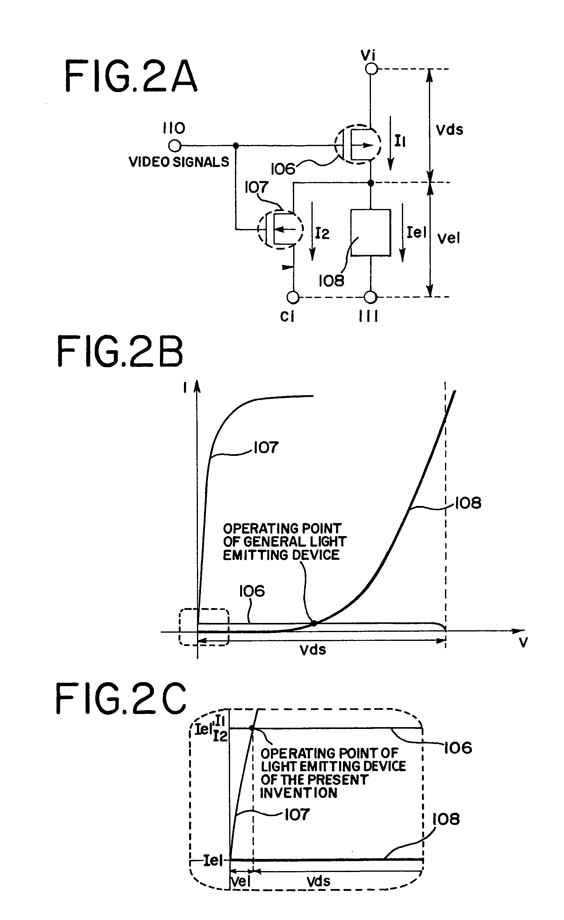
[0093]In this embodiment, the case where the light emitting device of the present invention as shown in FIGS. 1A and 1B is driven by a digital gradation system will be described using FIG. 6.

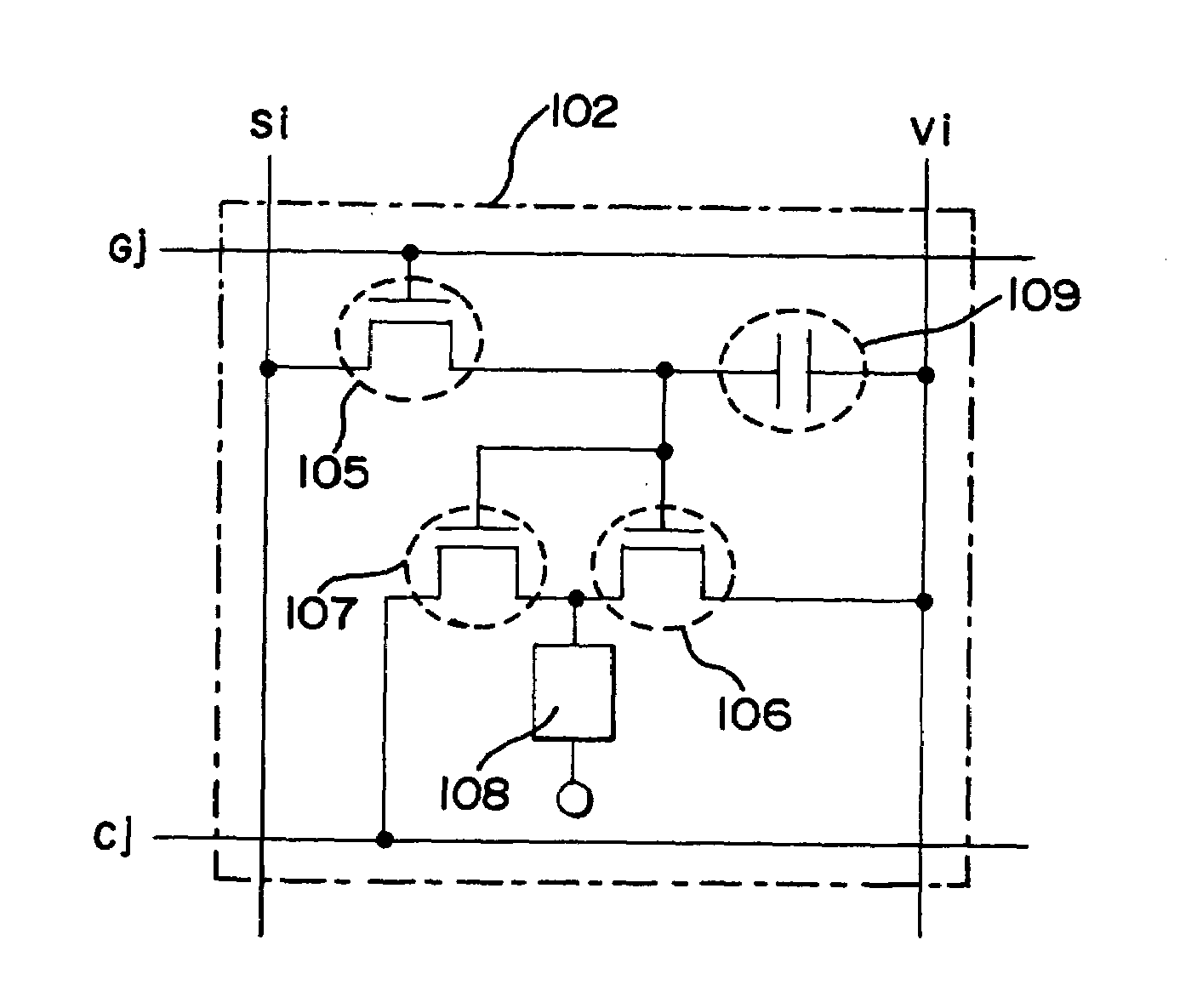
[0094]First, a potential of the counter electrode of the OLED is kept to be the same potential as a power source potential of the power source line. Then, the scan line G1 is selected by a selection signal inputted from the scan line driver circuit 104. As a result, the switching TFTs 105 of all pixels (pixels in the first line) connected with the scan line G1 become an on state.

[0095]Then, digital video signals of a first bit are inputted from the signal line driver circuit 103 to the signal lines (S1 to Sx). The digital video signals are inputted to the gate electrodes of the driver TFTs 106 and the gate electrodes of the discharging TFTs 107 through the switching TFT 105s.

[0096]Switchings of the driver TFTs 106 and the discharging TFTs 107 are controlled by information indicating 1 or 0, whi...

embodiment 2

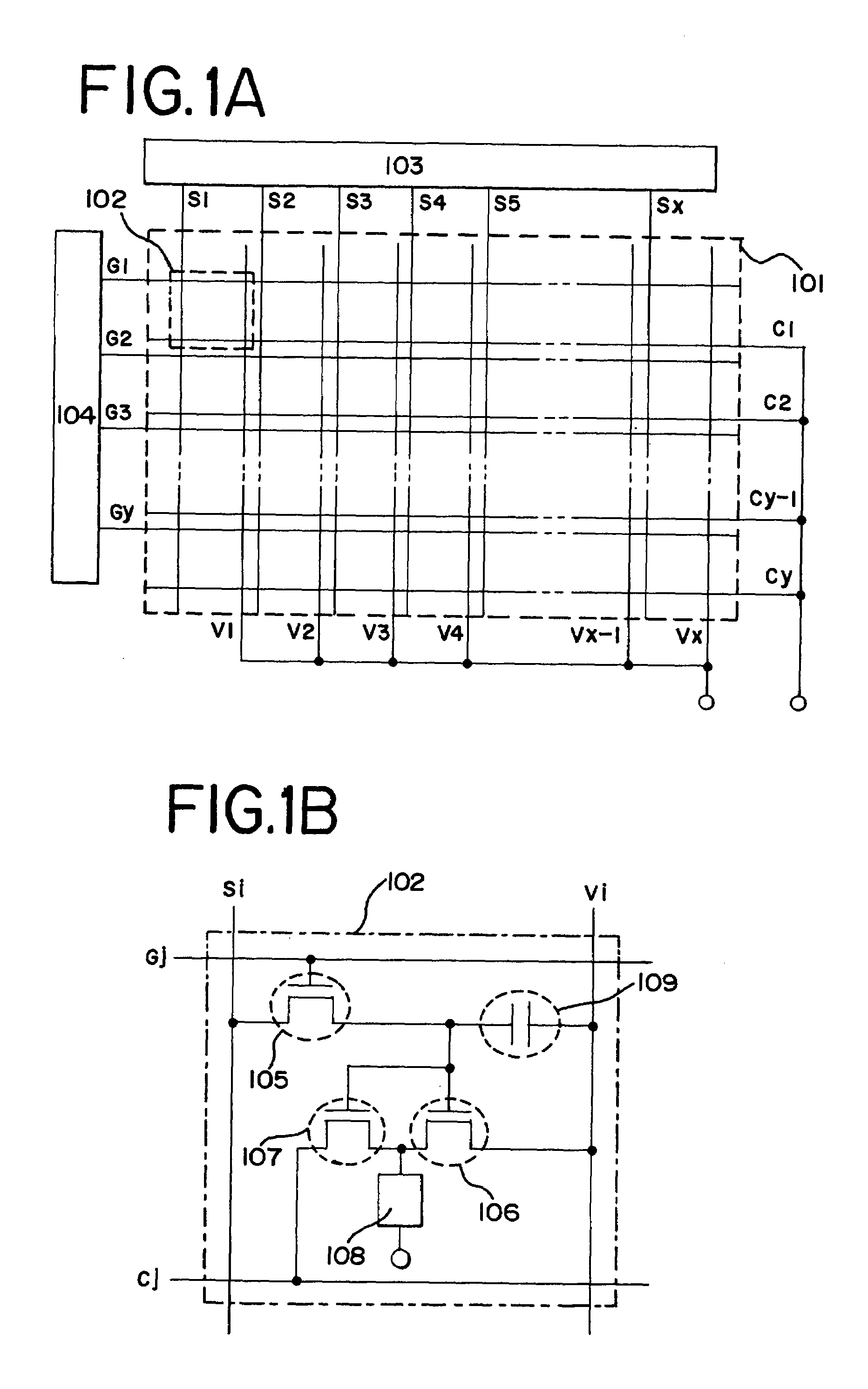
[0111]A structure of a pixel in the light emitting device of the present invention is not limited to the structure shown in FIG. 1B. In this embodiment, an example of a structure of a pixel in the light emitting device of the present invention, which is different from the structure shown in FIG. 1B, will be described. FIGS. 7A, 7B, 17A, and 17B show structures of a pixel in this embodiment.

[0112]A pixel shown in FIG. 7A includes at least one first signal line Sai, at least one second signal line Sbi, at least one first scan line Gaj, at least one second scan line Gbj, at least one power source line Vi, and at least one discharge line Cj.

[0113]Also, the pixel shown in FIG. 7A further includes a first switching TFT 705a, a second switching TFT 705b, a driver TFT 706, a discharging TFT 707, an OLED 708, and a storage capacitor 709.

[0114]Next, the connection among respective elements and wirings in the pixel shown in FIG. 7A will be described in more detail.

[0115]The gate electrode of t...

embodiment 3

[0160]Next, described with reference to FIGS. 8A to 12 is a method of forming the light emitting device of the present invention. Here, the method of simultaneously forming, on the same substrate, the switching TFT and the driver TFT of the pixel portion, and the TFTs of a driver portion provided surrounding the pixel portion is described in detail according to steps. Further, the method of forming the discharge TFT is not illustrated to simplify the explanation, because the discharge TFT can be formed by reference of manufacturing method of forming the switching TFT and the driver TFT.

[0161]This embodiment uses a substrate 900 of a glass such as barium borosilicate glass or aluminoborosilicate glass as represented by the glass #7059 or the glass #1737 of Corning Co. There is no limitation on the substrate 900 provided it has a property of transmitting light, and there may be used a quartz substrate. There may be further used a plastic substrate having heat resistance capable of wit...


PUM


Abstract

There is provided a light emitting device capable of preventing light emission of an OLED caused due to an off current of a driver TFT and suppressing a reduction in a contrast, to thereby display a beautiful image. A wiring which is kept at a predetermined potential (hereinafter referred to as a discharge line) is provided to make the off current flow into the discharge line rather than into the OLED. A TFT such as is turned on when the driver TFT is tuned off (hereinafter referred to as a discharging TFT) is provided in each pixel. With respect to the source region and the drain region of the discharging TFT, one is connected with a pixel electrode and the other is connected with the discharge line. According to the above structure, when the driver TFT is turned off, the discharging TFT is turned on. Thus, the off current in the driver TFT actively flows into the discharge line rather than into the OLED.

Description

BACKGROUND OF THE INVENTION[0001]1. Field of the Invention[0002]The present invention relates to an OLED (organic light emitting device) panel obtained by forming an OLED on a substrate and sealing the OLED between the substrate and a cover member. The invention also relates to an OLED module in which an IC including a controller, or the like, is mounted to the OLED panel. In this specification, light emitting device is the generic term for the OLED panel and for the OLED module. Electronic devices using the light emitting device are also included in the present invention.[0003]2. Description of the Related Art[0004]Being self-luminous, OLEDs eliminate the need for a backlight that is necessary in liquid crystal display devices (LCDs) and thus make it easy to manufacture thinner devices. Also, the self-luminous OLEDs are high in visibility and have no limitation in terms of viewing angle. These are the reasons for the attention that light emitting devices using the OLEDs are receivi...

Claims


Application Information

Patent Timeline
IPC IPC(8): G09G3/30G09G3/20G09G3/32
CPCG09G3/3233G09G3/3258G09G3/2022G09G2300/0426G09G2300/0842G09G2330/021G09G2310/0251G09G2310/0256G09G2320/0238G09G2320/043G09G2300/0861
Inventor KIMURA, HAJIME
Owner SEMICON ENERGY LAB CO LTD
Why Eureka
Try Eureka