Memory implementation for handling integrated circuit fabrication faults

Active Publication Date: 2006-06-13
INVENSAS CORP
View PDF4 Cites 6 Cited by
  • Summary
  • Abstract
  • Description
  • Claims
  • Application Information

AI Technical Summary

Benefits of technology

[0004]Advantages, features and objects of the present invention may include: (i) enabling a memory to be operative even though one or more memory cells may be faulty; (ii) providing a memory having a built-in fault-tolerant redundancy; (iii) increasing an effectiv

Problems solved by technology

It is often the case that integrated circuits with large amounts of on-chip RAM are vulnerable to fabrication errors when a small geometry fabrication process is used.
Fabrication yields can be unacce

Method used


Image

  • Memory implementation for handling integrated circuit fabrication faults
  • Memory implementation for handling integrated circuit fabrication faults
  • Memory implementation for handling integrated circuit fabrication faults

Examples


Embodiment Construction

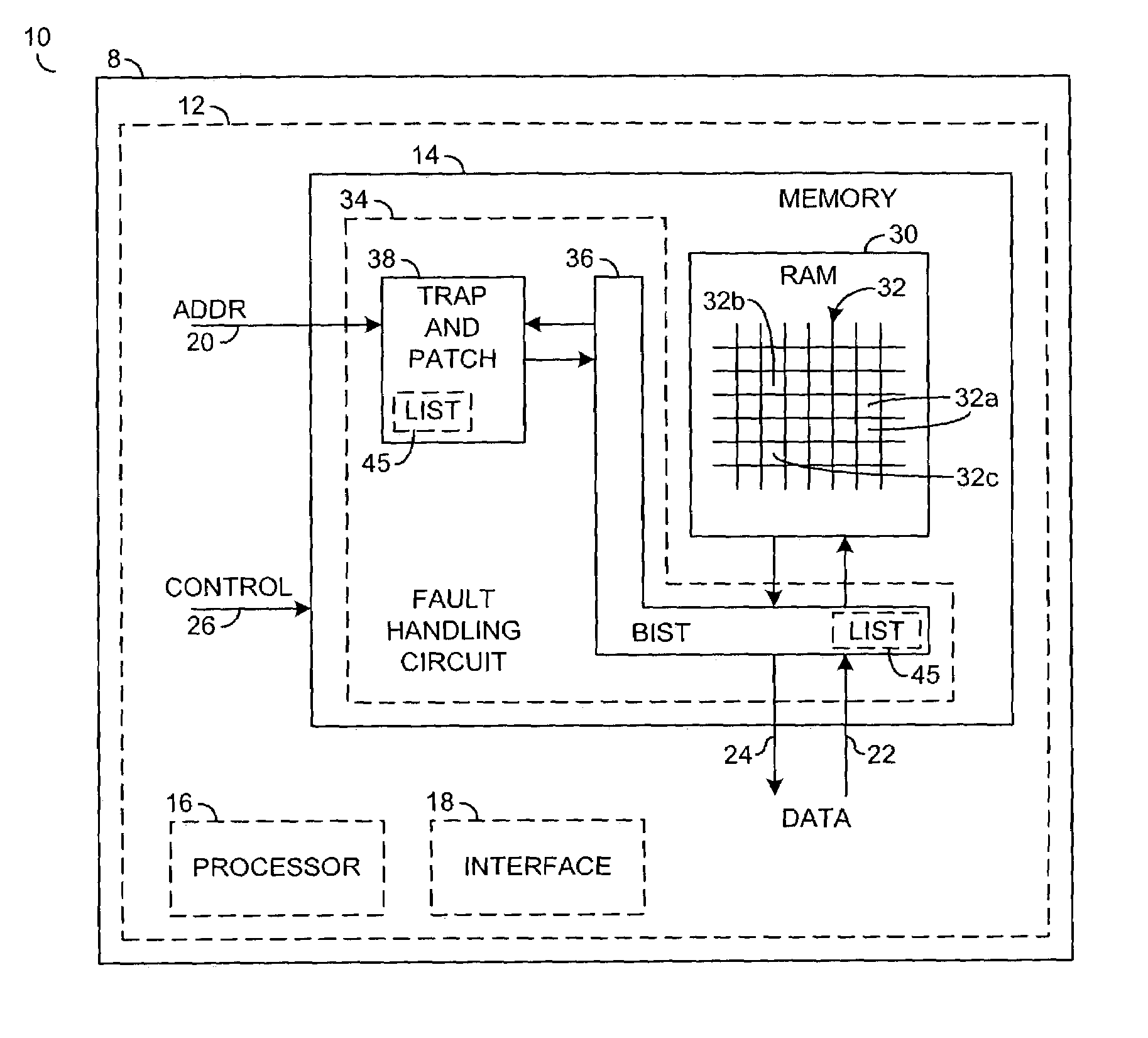
[0011]Referring to FIG. 1, an integrated circuit 10 may comprise a die 8 carrying circuitry 12 including built-in memory 14. The circuitry 12 may include other on-chip functional circuits, for example, a processor 16 and / or an interface circuit 18. The integrated circuit 10 may be a SoC circuit. The integrated circuit 10 may be an ASIC or an ASSP. The memory 14 may be an addressable RAM. Additionally or alternatively, the memory 14 may be a buffer. The buffer may be a first-in first-out (FIFO) buffer. The memory 14 may (i) interconnect first and second on-chip circuits (for example, the processor 16 and the interface circuit 18) within the integrated circuit 10, or (ii) be used to interconnect on-chip circuitry (for example, the processor 16 or the interface circuit 18) and off-chip circuitry (not shown). Although only a single region of memory 14 is illustrated in FIG. 1, the integrated circuit may include plural memories 14.

[0012]The memory 14 may generally be coupled to one or mo...


PUM


Abstract

The present invention may provide a circuit generally having a plurality of addressable memory cells and an access control circuit. The access control circuit may be configured to intercept an access to a faulty cell of the plurality of addressable memory cells. The access control circuit may be further configured to redirect the access to a spare cell of the plurality of addressable memory cells.

Description

FIELD OF THE INVENTION[0001]The present invention may relate to an implementation of memory within an integrated circuit. One aspect of the invention may relate to an implementation that may reduce the detrimental effect of a fabrication fault.BACKGROUND TO THE INVENTION[0002]Complicated system on a chip (SoC), application-specific integrated circuits (ASICs) and application-specific signal processors (ASSPS) often are large and employ significant amounts of on-chip random-access memory (RAM). Such a large circuit means that the smallest possible geometry fabrication process should be used to achieve a die size that is cost effective for manufacture. However, conventional bit cells of a RAM are optimised aggressively for a minimum cell area. It is often the case that integrated circuits with large amounts of on-chip RAM are vulnerable to fabrication errors when a small geometry fabrication process is used. Fabrication yields can be unacceptably low, especially while an immature fabr...

Claims


Application Information

Patent Timeline
IPC IPC(8): G01R31/28G11C29/00
CPCG11C29/76G11C29/808
Inventor TESTER, DAVID
Owner INVENSAS CORP
Why Eureka
Try Eureka