Method for making a semiconductor device having a high-k gate dielectric and a titanium carbide gate electrode

a technology of titanium carbide gate electrode and dielectric, which is applied in the direction of semiconductor devices, basic electric elements, electrical equipment, etc., can solve the problems of difficult to generate a titanium carbide layer with the desired thickness and workfunction using such a process

Inactive Publication Date: 2006-06-20
TAHOE RES LTD
View PDF38 Cites 64 Cited by
  • Summary
  • Abstract
  • Description
  • Claims
  • Application Information

AI Technical Summary

Problems solved by technology

Although an ALCVD process may be used to deposit such a layer on such a dielectric, it may be difficult to generate a titanium carbide layer with the desired thickness and workfunction using such a process.

Method used


Image

  • Method for making a semiconductor device having a high-k gate dielectric and a titanium carbide gate electrode
  • Method for making a semiconductor device having a high-k gate dielectric and a titanium carbide gate electrode
  • Method for making a semiconductor device having a high-k gate dielectric and a titanium carbide gate electrode

Examples


Embodiment Construction

[0007]A method for making a titanium carbide layer is described. That method comprises alternately introducing a carbon containing precursor and a titanium containing precursor at selected pulse times into a chemical vapor deposition reactor, while maintaining a substrate at a selected temperature. The reactor is operated for a sufficient time, and pulse times are selected for the carbon containing precursor and the titanium containing precursor, to form a titanium carbide layer of a desired thickness and workfunction on the substrate.

[0008]In the following description, a number of details are set forth to provide a thorough understanding of the present invention. It will be apparent to those skilled in the art, however, that the invention may be practiced in many ways other than those expressly described here. The invention is thus not limited by the specific details disclosed below.

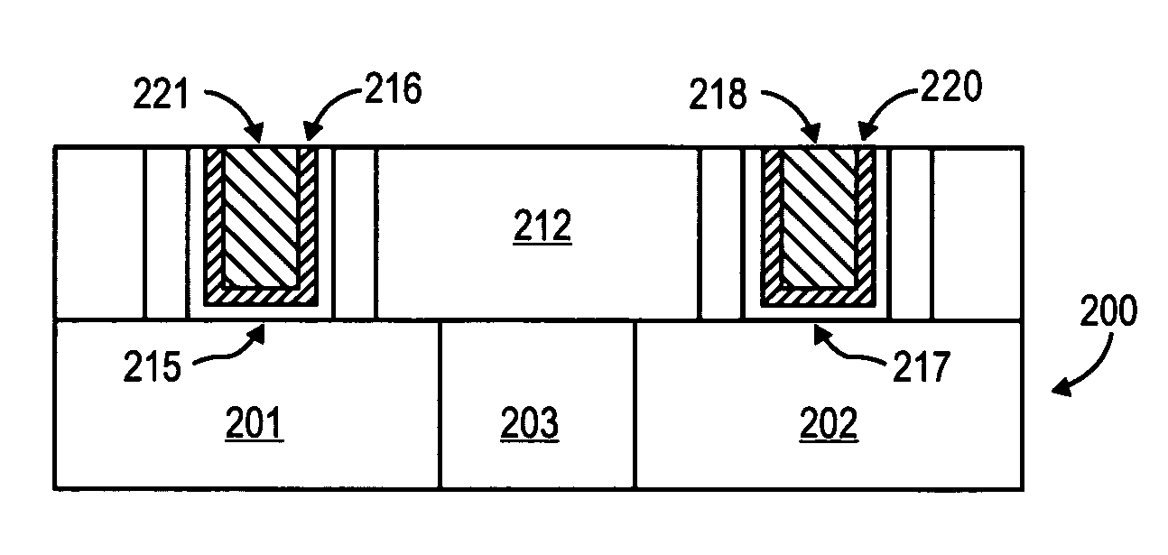
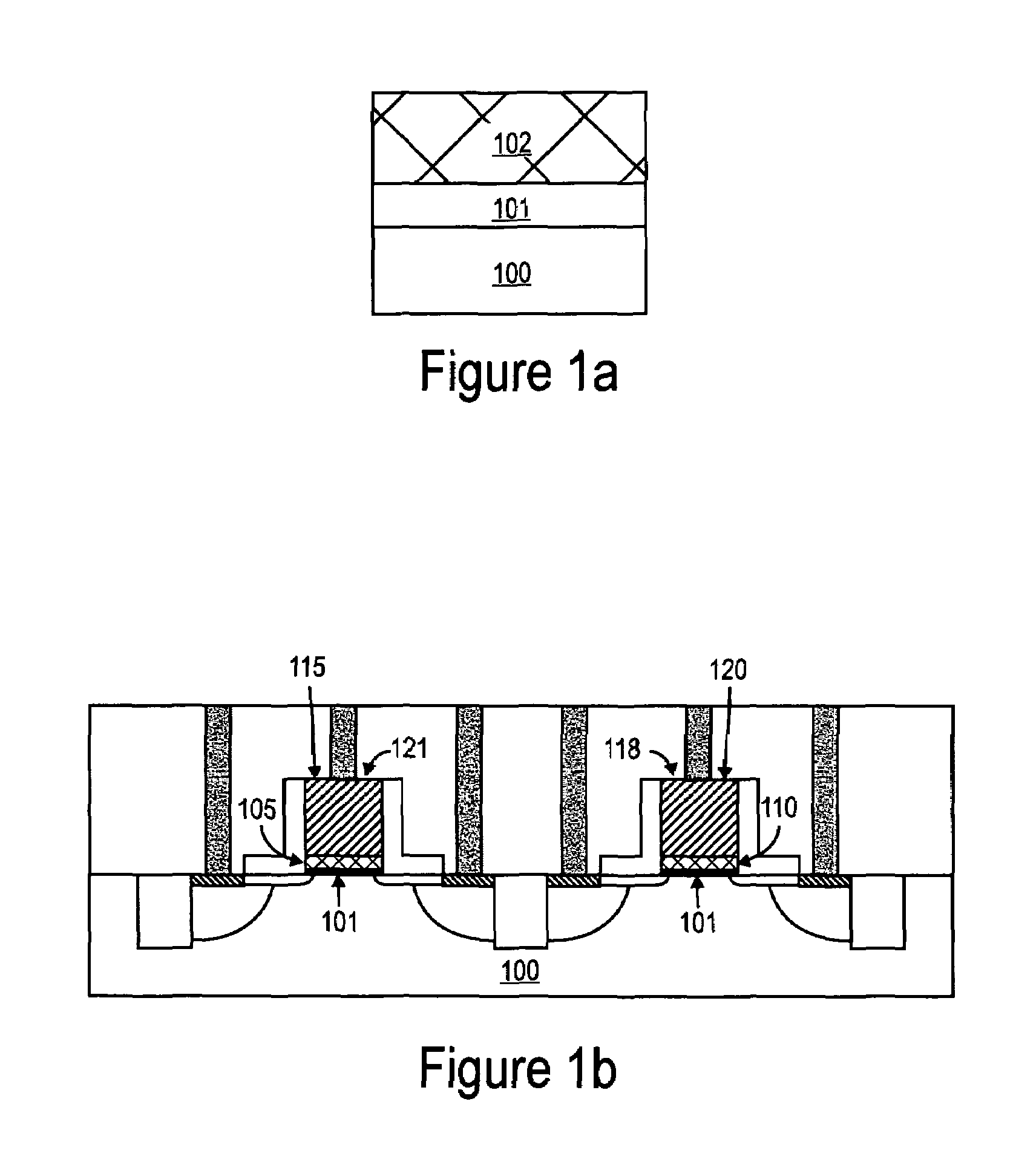
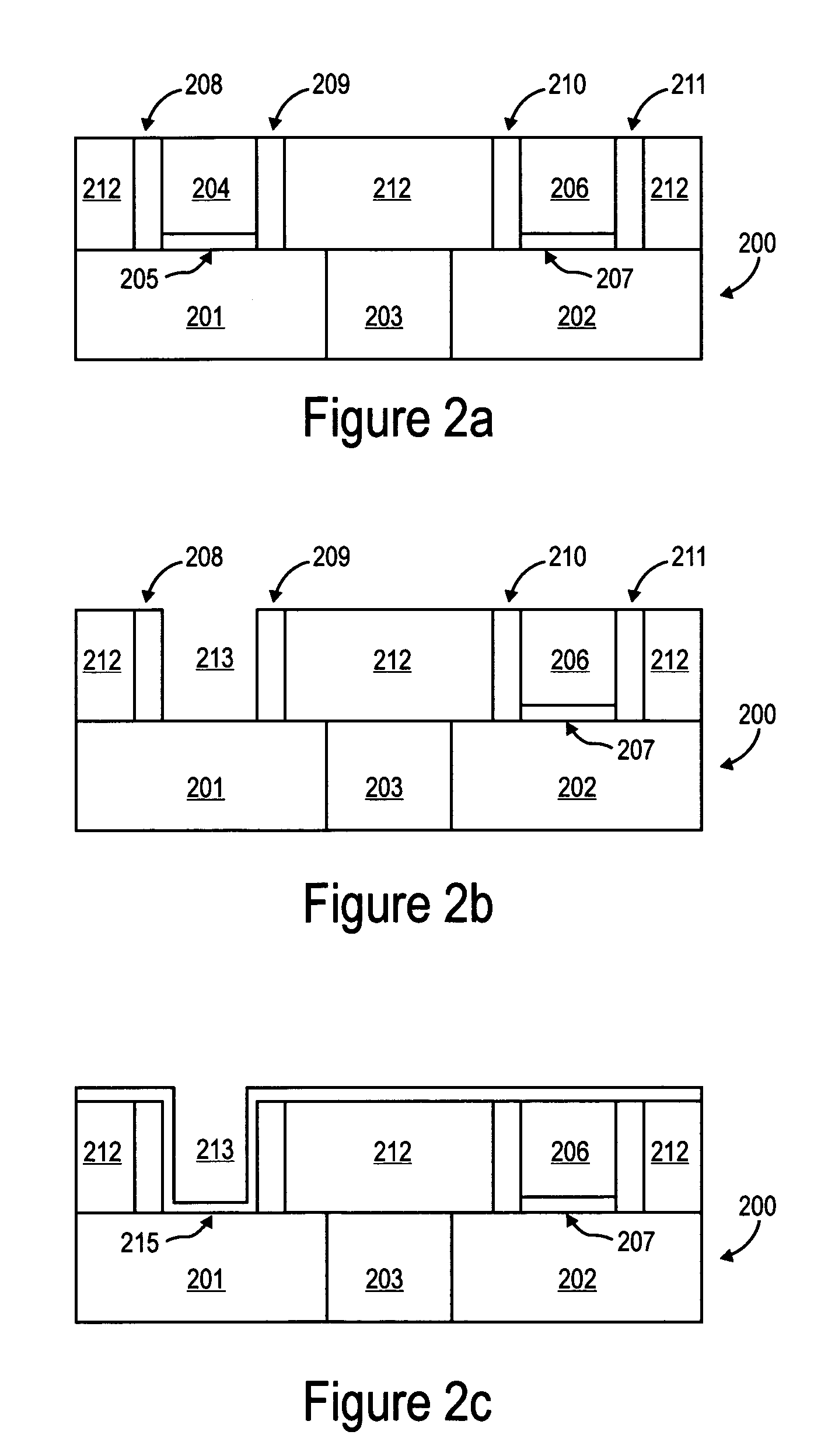
[0009]FIGS. 1a–1b represent cross-sections of structures that may be formed when carrying out an emb...


PUM

PropertyMeasurementUnit
temperatureaaaaaaaaaa
pulse timeaaaaaaaaaa

Abstract

A method for making a titanium carbide layer is described. That method comprises alternately introducing a carbon containing precursor and a titanium containing precursor into a chemical vapor deposition reactor, while a substrate is maintained at a selected temperature. The reactor is operated for a sufficient time, and pulse times are selected for the carbon containing precursor and the titanium containing precursor, to form a titanium carbide layer of a desired thickness and workfunction on the substrate.

Description

FIELD OF THE INVENTION[0001]The present invention relates to methods for making semiconductor devices, in particular, those with titanium carbide containing gate electrodes or barrier layers.BACKGROUND OF THE INVENTION[0002]An MOS field-effect transistor may include a high-k gate dielectric and a metal gate electrode. The metal gate electrode may comprise a titanium carbide layer, which may be formed on the high-k gate dielectric using an atomic layer chemical vapor deposition (“ALCVD”) process. Although an ALCVD process may be used to deposit such a layer on such a dielectric, it may be difficult to generate a titanium carbide layer with the desired thickness and workfunction using such a process.[0003]Accordingly, there is a need for an improved process for making a semiconductor device that includes a titanium carbide containing gate electrode or barrier layer. There is a need for an ALCVD process that may be tailored to produce a titanium carbide layer with the desired thickness...

Claims


Application Information

Patent Timeline
Patent Type & Authority Patents(United States)
IPC IPC(8): H01L21/44
CPCH01L21/28088H01L29/4966H01L21/823857H01L21/823842
Inventor METZ, MATTHEW V.DATTA, SUMANDOCZY, MARK L.KAVALIEROS, JACKBRASK, JUSTIN K.CHAU, ROBERT S.
Owner TAHOE RES LTD
Why Eureka
Try Eureka