
IC module and IC card

a technology applied in the field of ic modules and ic cards, can solve the problems of ic chips b>103/b> being damaged or broken, unable to absorb all the electrostatic stress caused by static electricity, and unable to absorb static electricity. , to achieve the effect of facilitating the process and enabling the strength of ic cards with respect to bending

Inactive Publication Date: 2006-06-20
SHARP KK
View PDF9 Cites 21 Cited by
  • Summary
  • Abstract
  • Description
  • Claims
  • Application Information

AI Technical Summary

Benefits of technology

The present invention provides an IC module and an IC card that can secure strength against bending and protect the IC chip from static electricity. The IC module includes an IC chip and a terminal group provided on a substrate, with a ground terminal and other terminals positioned close to each other. This arrangement ensures a constant gap between the ground terminal and other terminals, allowing for a discharge path for surge discharge. The IC card includes the IC module, providing high strength against bending and protecting the IC chip from static electricity. The invention also provides a simple structure for the IC card, making it easier and less expensive to manufacture.

Problems solved by technology

However, when the electrostatic strength is not allowable for the IC chip 103, it is impossible to absorb all the electrostatic stress caused by the static electricity, so that an input / output terminal (not shown) of the IC chip 103 is damaged or broken.
When an excessive voltage protection element (ESD protection circuit) provided in a general IC chip 103 cannot allow the special impulse current component, the IC chip 103 is damaged or broken.
Taking into consideration the impulse current component contained in the surge component in this manner, the structure of the IC module recited in the Patent Document 1 is not effective in protecting the IC chip from the ESD.
Further, high accuracy is required in processing the plurality of metal protruding portions so that a terminal distance therebetween is less than 100 μm, and this causes productivity to drop.
As a result, the end of the protruding portion tends to be damaged.
Thus, it is considered that: a shape of each input / output contact terminal 302 of the IC module recited in the Patent Document 1 is disadvantageous in using the IC card.
This is likely to result in chip breakage.
When the NC terminal is provided on the IC module, the IC chip is more likely to be damaged or broken than the IC module having no NC terminal.
Thus, it can be said that the IC chip is highly likely to be damaged or broken by the special impulse current component contained in the surge discharge component.

Method used


Image

  • IC module and IC card
  • IC module and IC card
  • IC module and IC card

Examples


embodiment 1

[Embodiment 1]

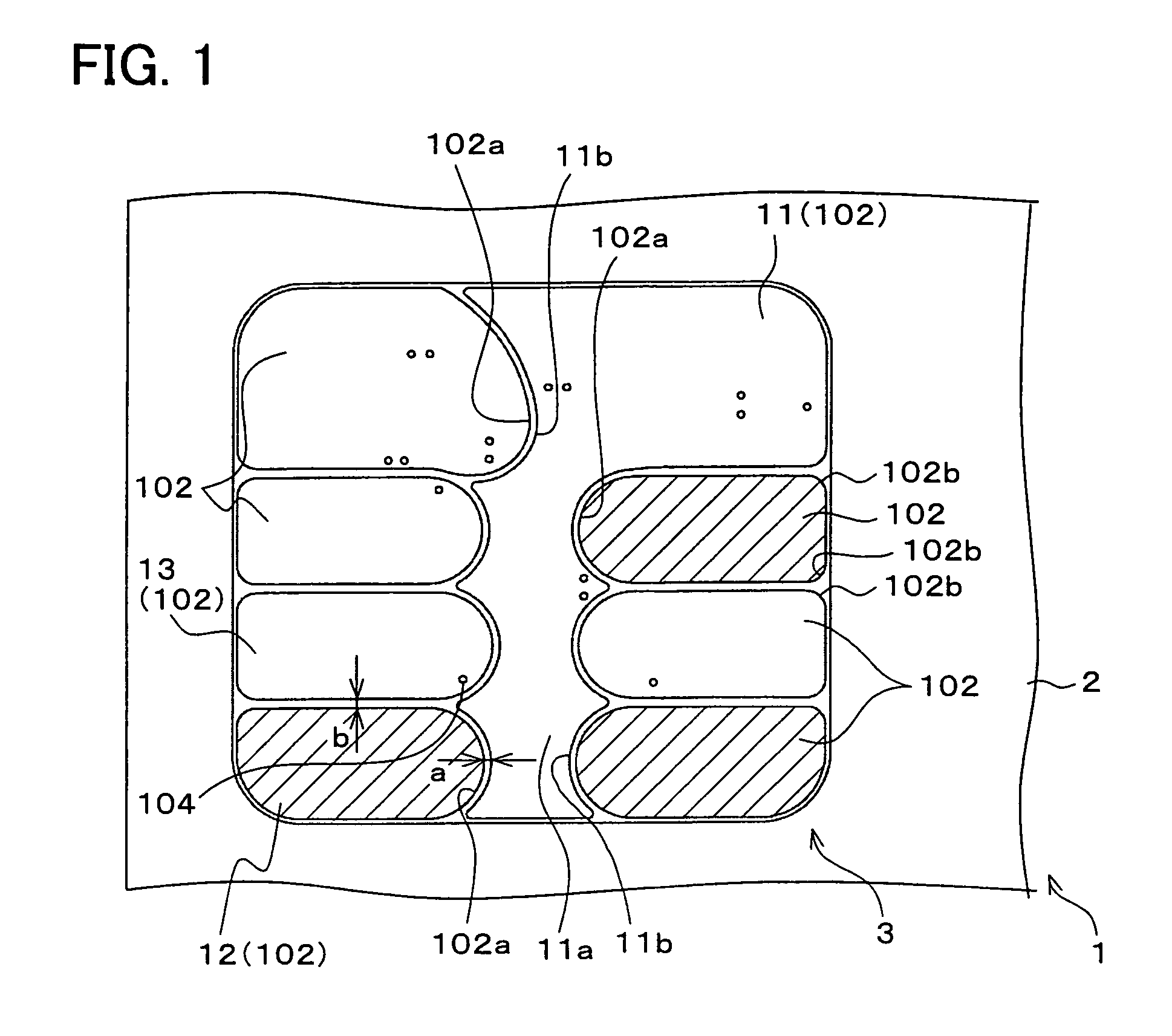
[0072]The following description explains one embodiment of the present invention with reference to FIGS. 1 to 5, FIG. 9, FIG. 10, and FIGS. 14 to 18. Note that, for convenience in description, the same reference signs are given to components having the same functions as components of the conventional IC module, and description thereof is omitted. Note that, the following embodiment explains a case where the IC module is provided on an IC card as an example, but the present invention is not limited to this.

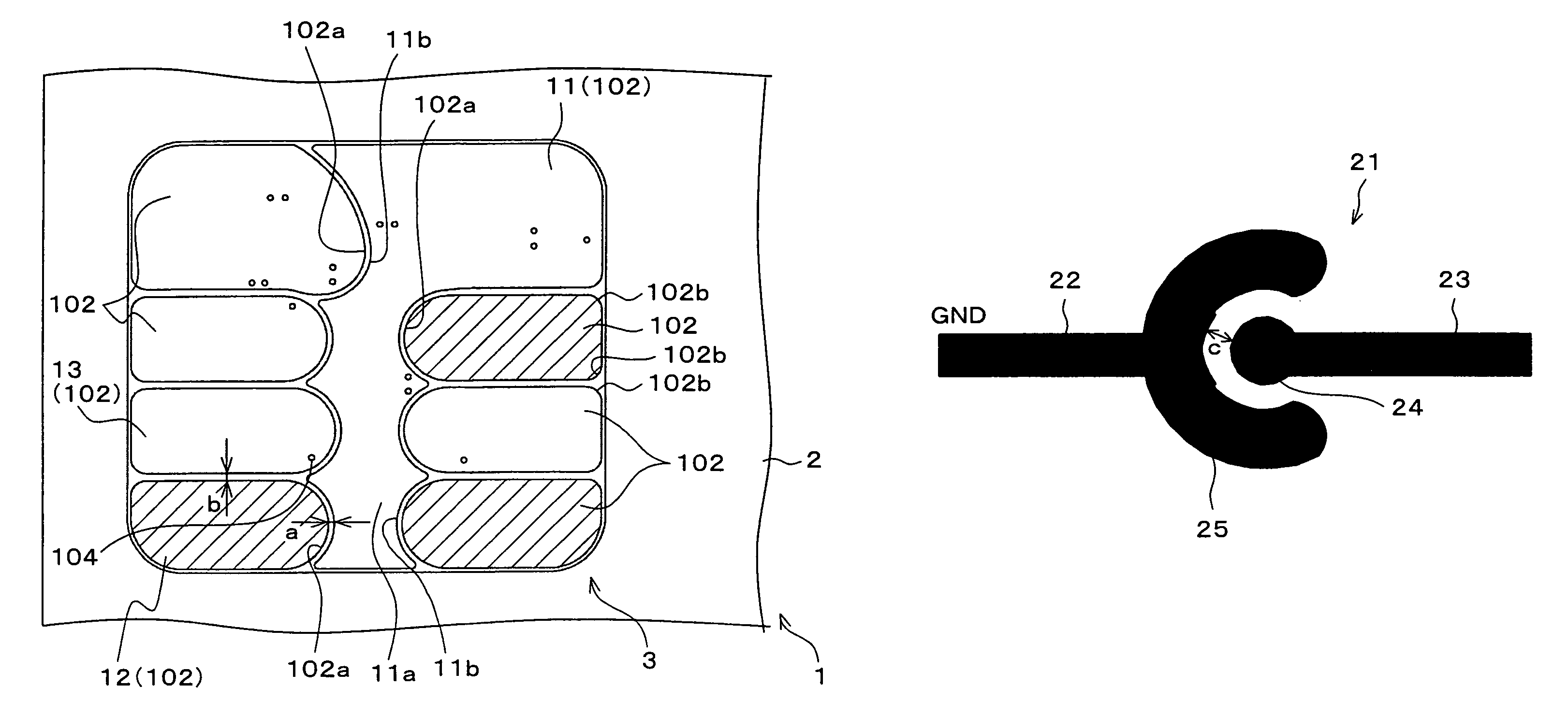
[0073]FIG. 1 schematically shows an arrangement of an IC module formation portion of the IC card according to the present embodiment. Further, FIG. 14 schematically shows an arrangement of the IC card according to the present embodiment. FIG. 5 schematically shows an important portion of the IC card shown in FIG. 14. In the present embodiment, a contact type IC card is described as an example of the IC card, but arrangements of the IC module and the IC card according ...

embodiment 2

[Embodiment 2]

[0132]The following description explains another embodiment of the present invention with reference to mainly FIG. 6 to FIG. 8. The present embodiment explains mainly differences from Embodiment 1. Note that, for convenience in description, the same reference signs are given to components having the same functions as components of the conventional IC module and the IC module according to Embodiment 1, and description thereof is omitted.

[0133]Embodiment 1 describes the case of improving a shape of the contact terminal 102, provided on the insulating support substrate 101 so as not to be positioned on a surface having no IC chip 103, so as to improve the strength with respect to the electrostatic discharge (ESD). The present embodiment describes mainly a case of improving a terminal shape of a wiring pattern, provided on the insulating support substrate 101 so as to be positioned on the surface where the IC chip 103 is provided (mounted), so as to improve the strength wi...


PUM


Abstract

Each of contact terminals, provided on a substrate of an IC module so as to be positioned on a back surface of a surface having an IC chip, which are terminals other than a GND terminal, has a curved convex face, and the GND terminal has a curved concave face as a counter face opposite to the curved convex face of the contact terminal so that there is a constant gap between the curved convex face and the curved concave face, and a gap between the GND and each of the contact terminals other than the GND terminal is narrower than a gap between all the contact terminals other than the GND terminal provided on the substrate so as to be positioned on the back surface of the surface having the IC chip. Thus, it is possible to provide an IC module and an IC card each of which enables the IC card's strength with respect to bending to be secured, and facilitates process thereof, and enables the IC chip to be protected from static electricity.

Description

[0001]This Nonprovisional application claims priority under 35 U.S.C. § 119(a) on Patent Application Ser. No. 2003 / 195278 filed in Japan on Jul. 10, 2003, the entire contents of which are hereby incorporated by reference.FIELD OF THE INVENTION[0002]The present invention relates to (i) a so-called IC module, i.e., a semiconductor device in which: an IC chip is electrically connected to a print wiring substrate, and an external connection terminal for allowing electrical connection with outside is provided on the print wiring substrate so as to be positioned on a back surface of a surface having the IC chip, and to (ii) an IC card having the IC module. More specifically, the present invention relates to an IC module and an IC card each of which is arranged so that an IC chip included therein is protected from static electricity.BACKGROUND OF THE INVENTION[0003]An IC module is a semiconductor device in which: an IC (integrated circuit) chip is electrically connected to a substrate such...

Claims


Application Information

Patent Timeline
Patent Type & Authority Patents(United States)
IPC IPC(8): H01L23/02G06K19/06H01K1/14B42D15/10G06K19/07G06K19/077H01L23/12H01L23/498H01L23/62H05K7/00
CPCG06K19/07728G06K19/07743G06K19/07747H01L23/49855H01L23/62H01L2924/12041H01L2924/01019H01L24/49H01L24/48H01L2224/48227H01L2224/49171H01L2924/01079H01L2924/19041H01L2924/00H01L24/45H01L2224/451H01L2224/45124H01L2224/45144H01L2924/00014H01L2924/14H01L2924/181H01L2224/05599H01L2924/00012
Inventor OKITA, YOSHITAKANISHIKAWA, MASATAKA
Owner SHARP KK
Learn More