Non-volatile semiconductor memory device using differential start programming voltage and programming method thereof

a semiconductor memory and programming voltage technology, applied in static storage, digital storage, instruments, etc., can solve the problems of difficulty in reducing and the number of programming loops appears relatively large, so as to reduce the dispersion of the number of programming loops related to an overall programming operation, reduce and achieve the effect of reducing the number of programming loops

Active Publication Date: 2006-06-20
SAMSUNG ELECTRONICS CO LTD
View PDF8 Cites 72 Cited by
  • Summary
  • Abstract
  • Description
  • Claims
  • Application Information

AI Technical Summary

Benefits of technology

[0011]Another feature of the present invention is to provide a non-volatile semiconductor memory device having a programming circuit, which is capable of reducing dispersion for the number of programming loops.
[0020]That is, according to the present invention, the number of programming loops is reduced even for a word line having a relatively large loading, thus a dispersion for the number of programming loops related to an overall programming operation is reduced. Therefore, a high-speed programming operation and an operating efficiency can be obtained.

Problems solved by technology

However, since positions or architectures of word lines within a memory cell block are not same as one another, dispersion for the number of programming loops appears relatively large.
Thus, there is a difficulty in reducing the dispersion for the number of programming loops.

Method used


Image

  • Non-volatile semiconductor memory device using differential start programming voltage and programming method thereof
  • Non-volatile semiconductor memory device using differential start programming voltage and programming method thereof
  • Non-volatile semiconductor memory device using differential start programming voltage and programming method thereof

Examples


Embodiment Construction

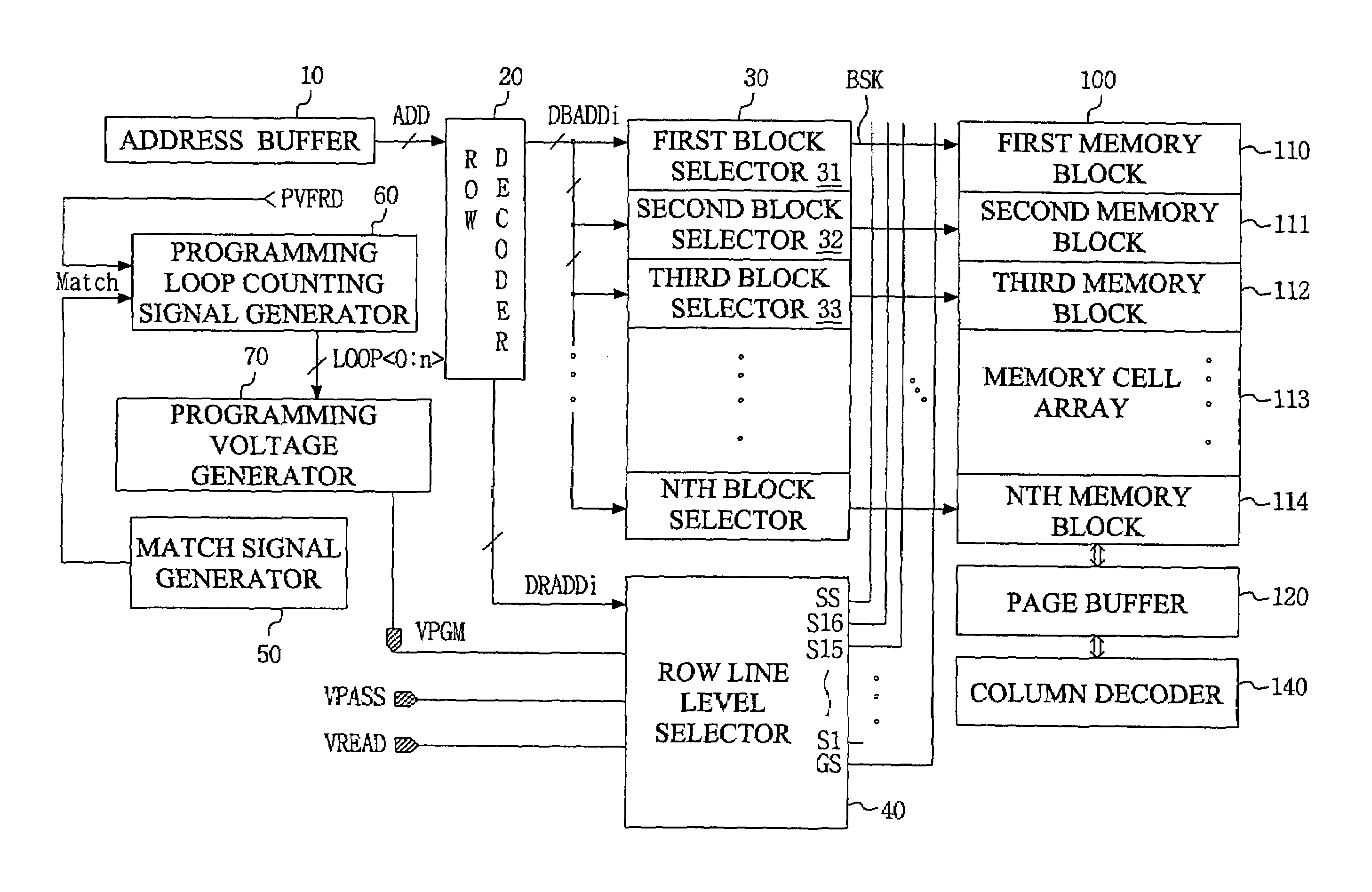
[0034]According to exemplary embodiments of the present invention, a non-volatile semiconductor memory device using a differential start programming voltage, and a programming method thereof, will be described with reference to the accompanied drawings.

[0035]It will be understood by those skilled in the art that the present invention can be embodied by numerous different types and is not limited to the following described embodiments. The following various embodiments are exemplary in nature. Accordingly, details of like components have been omitted so that the invention can be clearly presented, and like components have like reference symbols and numerals.

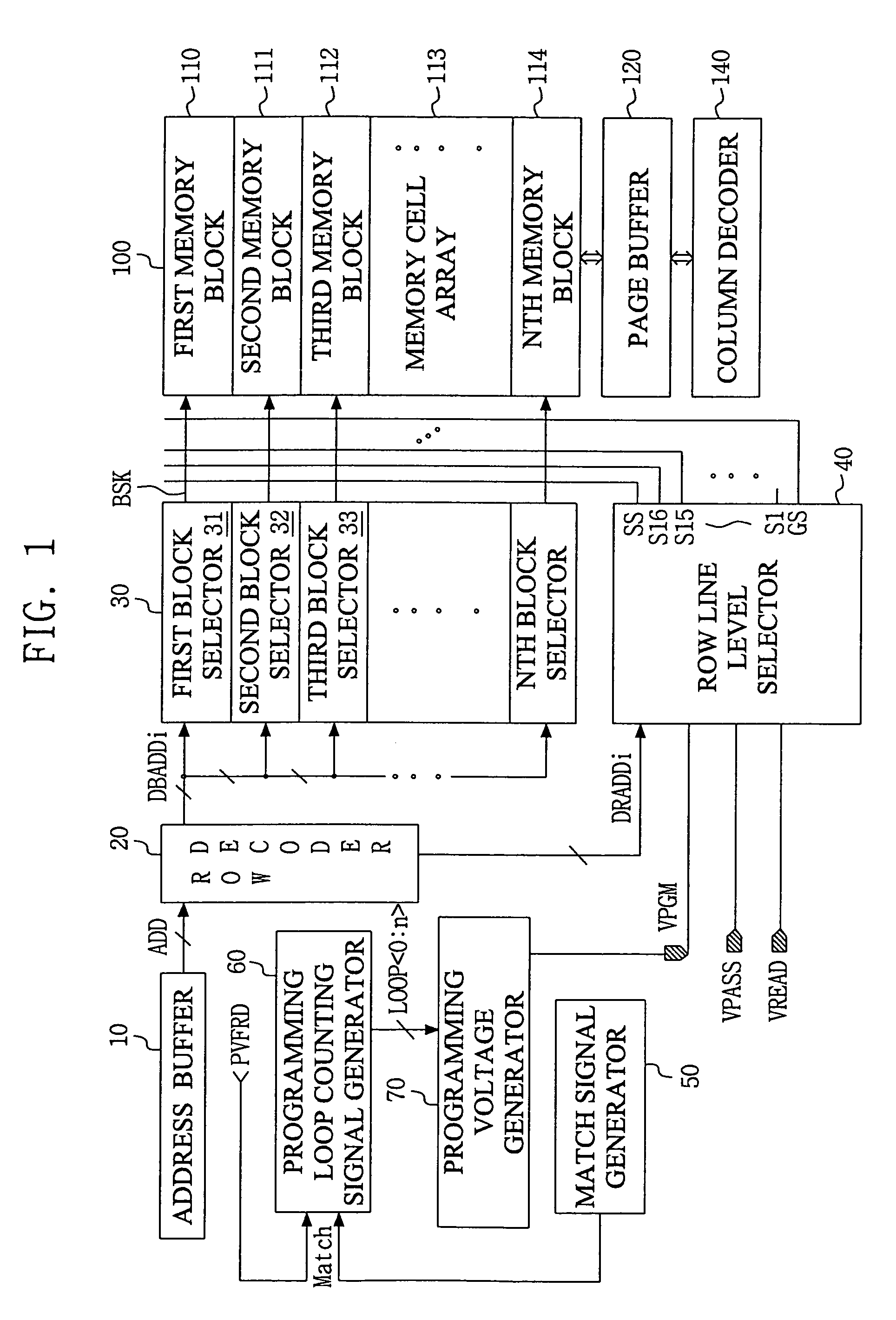
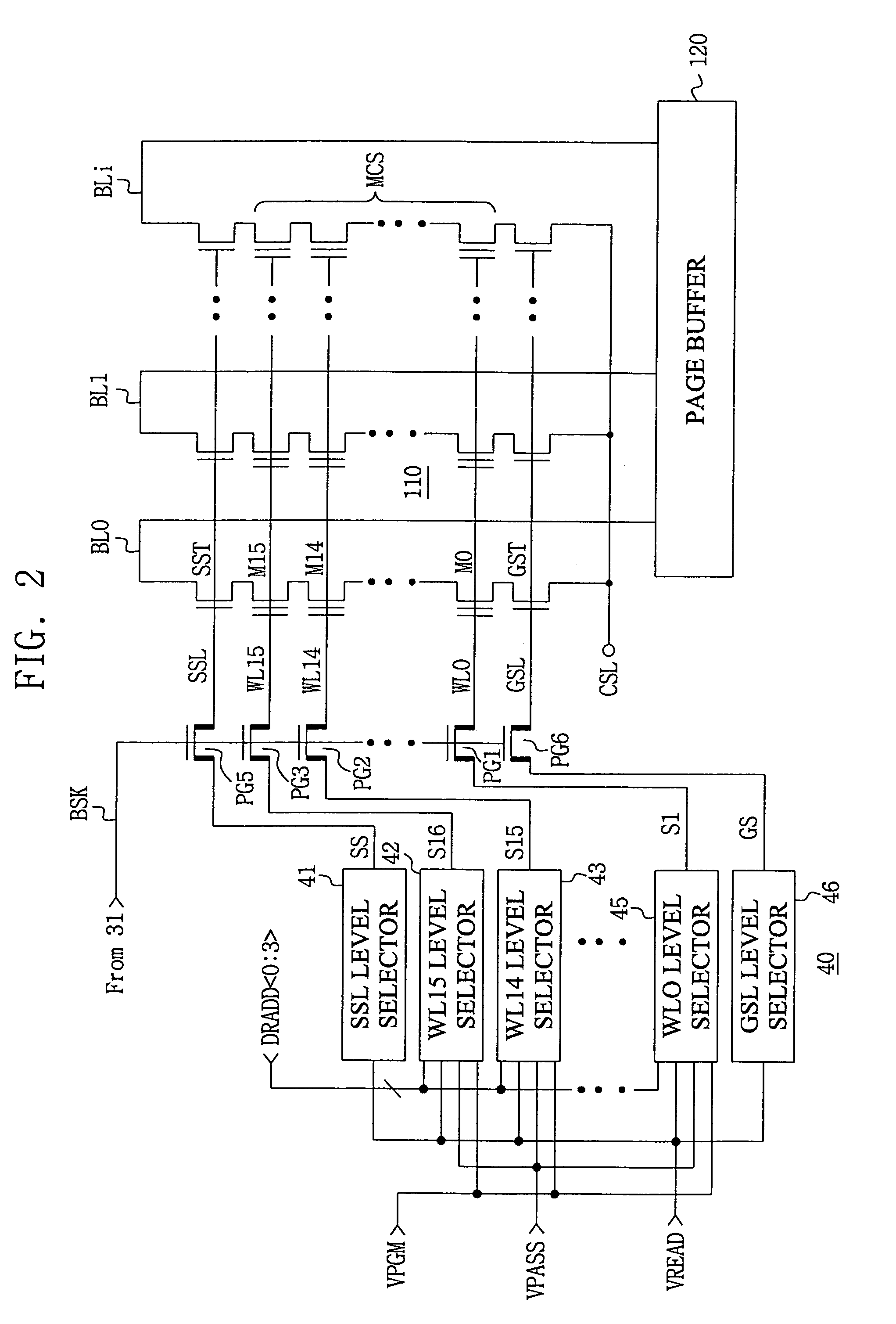
[0036]FIG. 1 is a block diagram of non-volatile semiconductor memory device according to an exemplary embodiment of the present invention. FIG. 2 is a circuit diagram showing a detailed connection relationship between a memory block 110 and a row line level selector 40 referred to FIG. 1. FIG. 3 is an exemplary circuit diagram sho...


PUM


Abstract

In a non-volatile semiconductor memory device which differentially uses a start programming voltage during a programming operation mode in order to reduce a dispersion for the number of programming loops, the programming method includes previously storing a row address that indicates at least one specific word line among a plurality of word lines; and applying a start programming voltage to the specific word line, when a row address applied in a programming operation mode coincides with the stored row address, the start programming voltage having a level that is different from a level of start programming voltage to be applied to the rest word lines except the specific word line, whereby reducing dispersion for the programming loop number and realizing a high-speed programming operation and operating efficiency.

Description

CROSS REFERENCE TO RELATED APPLICATION[0001]This application claims priority under 35 USC § 119 to Korean Patent Application No. 2003-100108, filed on Dec. 30, 2003, the contents of which are herein incorporated by reference in their entirety for all purposes.FIELD OF THE INVENTION[0002]The present invention relates to a non-volatile semiconductor memory device, and particularly, to a non-volatile semiconductor memory device having a programming circuit for programming a memory cell having a floating gate, and a programming method thereof.PRIOR ART OF THE INVENTION[0003]A non-volatile semiconductor memory device such as a flash EEPROM (electrically erasable programmable read only memory) etc. is generally widely known as a data storage device of portable electronic system. A NAND flash semiconductor memory device having a memory cell array of NAND cell type is widely known in this field as a memory where integration of memory cells is relatively prominent and a flash is erasable. In...

Claims


Application Information

Patent Timeline
Patent Type & Authority Patents(United States)
IPC IPC(8): G11C16/00G11C11/34G11C16/02G11C16/04G11C16/06G11C16/08G11C16/10G11C16/12G11C16/34
CPCG11C16/0483G11C16/3418G11C16/12G11C16/08G11C16/02
Inventor LEE, KYEONG-HANLEE, JUNE
Owner SAMSUNG ELECTRONICS CO LTD
Why Eureka
Try Eureka