
Phase-change memory devices

a memory device and phase-change technology, applied in the field of phase-change memory devices, can solve the problems of increasing the difficulty of reducing the program current in such devices, limiting the diameter of the bottom electrode b>13/b>, and limiting the amount of program current to be reduced

Inactive Publication Date: 2006-06-27
SAMSUNG ELECTRONICS CO LTD
View PDF6 Cites 107 Cited by
  • Summary
  • Abstract
  • Description
  • Claims
  • Application Information

AI Technical Summary

Benefits of technology

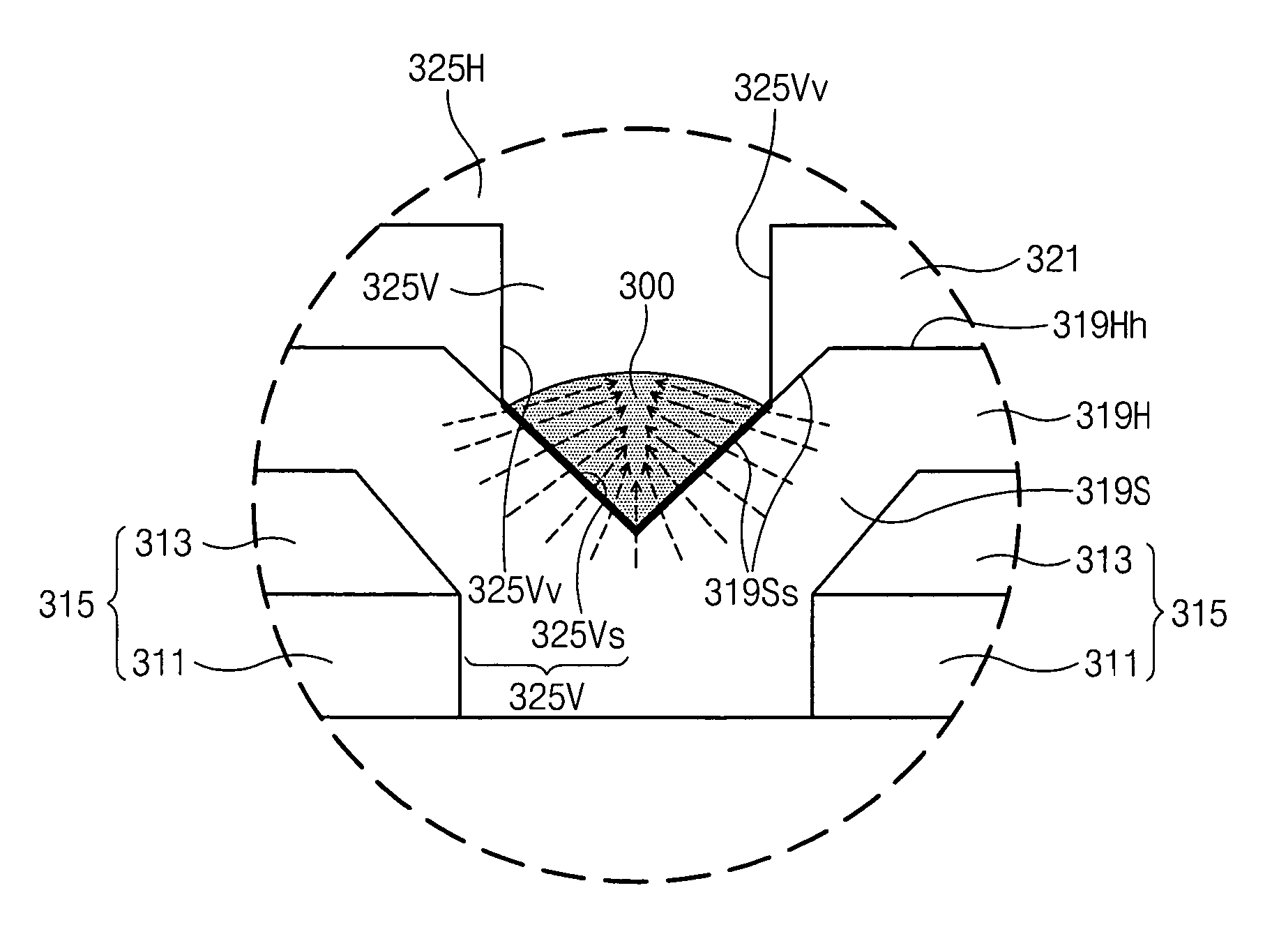
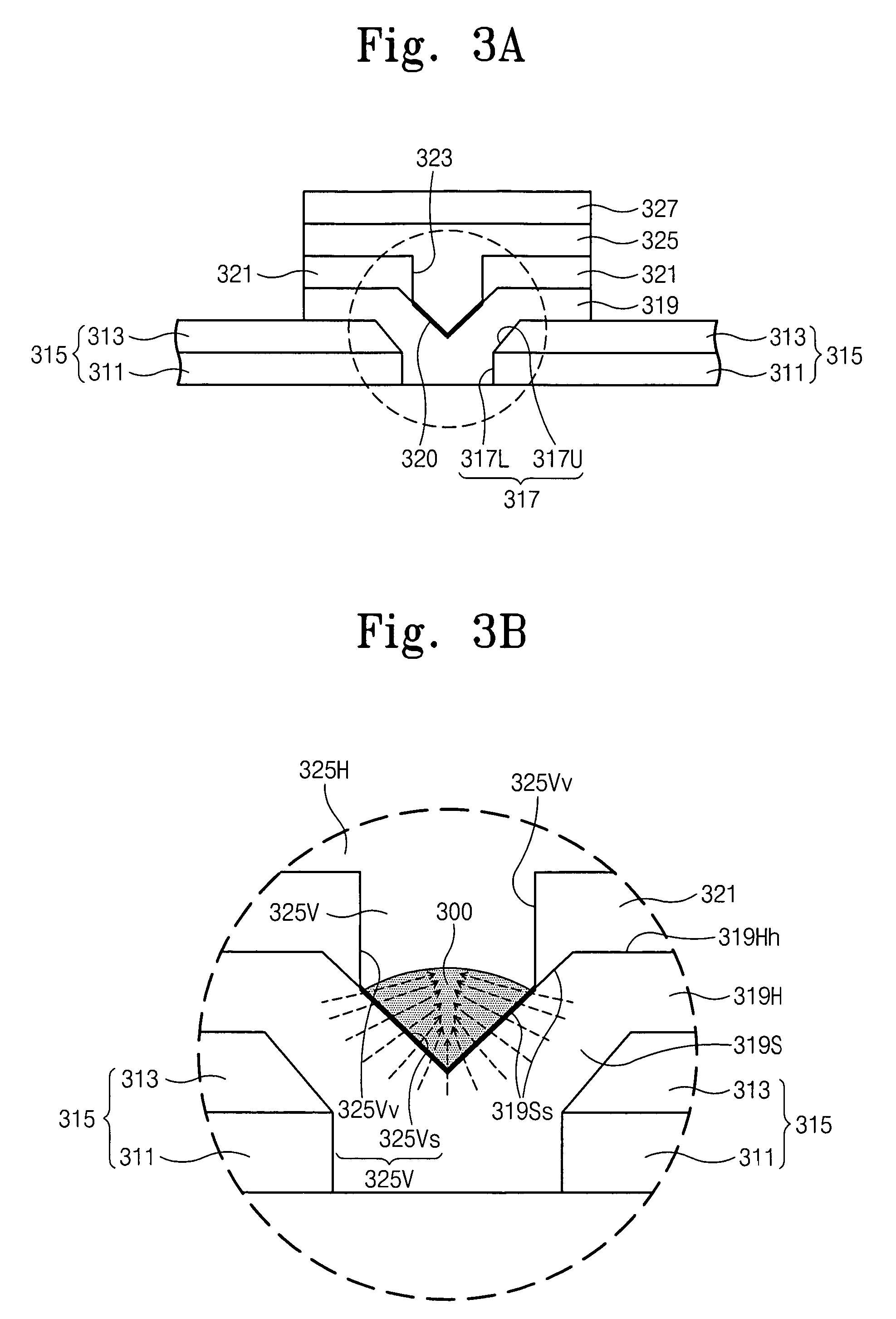
The present invention provides phase-change memory devices with improved current density concentration at the contact area between the first electrode and the phase-change material layer. This is achieved by including a tapering tip of the phase-change material layer that contacts the first electrode at the contact area. The phase-change material layer also includes a horizontal part extending above the vertical part of the first electrode. The first electrode may have a recess in the contact area. The phase-change material layer may also include a second electrode on the horizontal part of the first electrode. The invention also provides methods for fabricating the phase-change memory devices.

Problems solved by technology

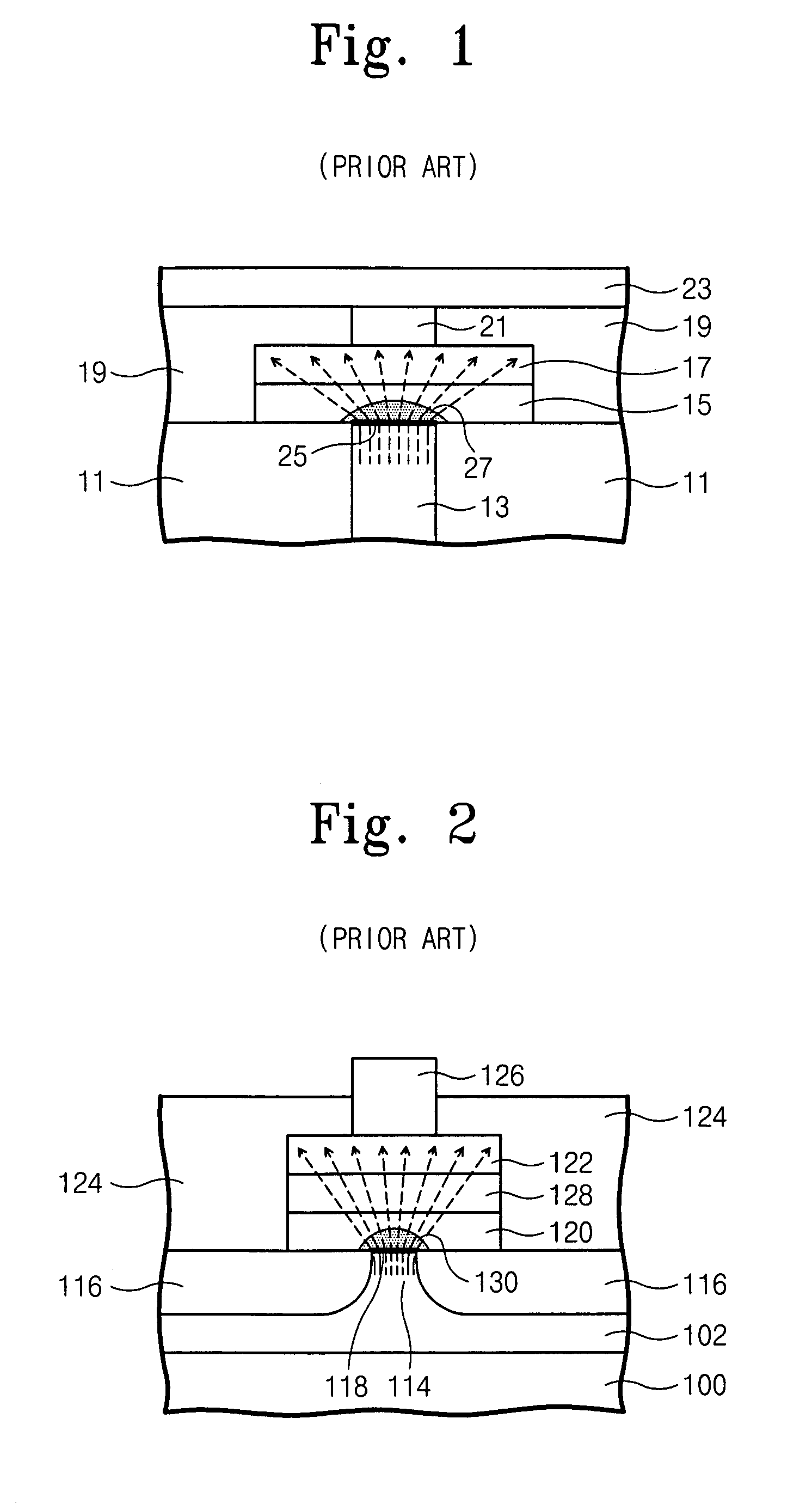
However, the diameter of the bottom electrode 13 may be limited by a resolution of a photolithography process used in forming the bottom electrode 13.
As a result, there is generally a limit to how much the program current may be reduced by this approach.
As a result, current density generally decreases as the current passes through the phase-change material layer, which may increase the difficulty of reducing the program current in such devices.

Method used


Image

  • Phase-change memory devices
  • Phase-change memory devices
  • Phase-change memory devices

Examples


Embodiment Construction

[0037]The present invention now will be described more fully hereinafter with reference to the accompanying drawings, in which embodiments of the invention are shown. This invention may, however, be embodied in many different forms and should not be construed as limited to the embodiments set forth herein. Rather, these embodiments are provided so that this disclosure will be thorough and complete, and will fully convey the scope of the invention to those skilled in the art. In the drawings, the relative sizes of regions may be exaggerated for clarity. It will be understood that when an element is referred to as being “attached”, “connected,”“on” or “coupled” to another element, it can be directly connected or coupled to or on the other element or intervening elements may be present. In contrast, when an element is referred to as being “directly attached,”“directly connected,”“directly on” or “directly coupled” to another element, there are no intervening elements present. Like numb...


PUM


Abstract

Phase-change memory devices include a phase-change material layer and a first electrode having a contact area therebetween. The contact area extends into a recess of the first electrode to provide current density concentration.

Description

CLAIM OF PRIORITY[0001]This application claims priority from Korean Patent Application No. 2003-20755, filed on Apr. 2, 2003, in the Korean Intellectual Property Office, the disclosure of which is hereby incorporated herein by reference.BACKGROUND OF THE INVENTION[0002]The present invention relates to integrated circuit (semiconductor) memory devices and more specifically, to phase-change memory devices and methods for forming the same.[0003]Semiconductor memory devices are generally classified as volatile memory devices or as non-volatile memory devices, based on whether data can be maintained when power to the device is turned off. Examples of a volatile memory device include a dynamic random access memory (DRAM) or a static random access memory (SRAM). An example of a non-volatile memory device is a FLASH memory. In such memory devices, stored binary information, having a “0” or a “1” state, may be determined by sensing a stored charge in a memory cell.[0004]Investigations contin...

Claims


Application Information

Patent Timeline
Patent Type & Authority Patents(United States)
IPC IPC(8): H01L47/00H01L29/04H01L27/10H01L21/00H10N80/00H01L27/24
CPCH01L27/2436H01L45/06H01L45/1683H01L45/1273H01L45/144H01L45/1233H10B63/30H10N70/231H10N70/8418H10N70/826H10N70/8828H10N70/066H01L27/10
Inventor HWANG, YOUNG-NAMKIM, YOUNG-TAE
Owner SAMSUNG ELECTRONICS CO LTD
Learn More