Multi-layer integrated semiconductor structure having an electrical shielding portion

a semiconductor structure and integrated technology, applied in semiconductor devices, semiconductor/solid-state device details, electrical apparatus, etc., can solve problems such as electrical noise or interference, parametric interactions, and electrical noise or interference between large complex digital circuits, and achieve the effect of reducing interferen

Inactive Publication Date: 2006-06-27
MASSACHUSETTS INST OF TECH
View PDF47 Cites 193 Cited by
  • Summary
  • Abstract
  • Description
  • Claims
  • Application Information

AI Technical Summary

Benefits of technology

[0010]With this particular arrangement, a multi-layer integrated semiconductor structure capable of having mixed-signal circuits is provided. The proposed isolation structure can be effectively integrated in a mixed-technology application. For example, the first semiconductor device layer may correspond to a digital technology; whereas, the second device layer is fabricated using an analog technology. The isolation structure would substantially reduce the interference generated by the digital layer and its effect on the sensitive analog circuits.

Problems solved by technology

However, one of the most significant problems to the realization of an SOC is the parasitic interactions (e.g. electrical noise or interference) between large complex digital circuits and highly sensitive analog circuits.
Substrate noise can be a significant interferer.
The noise coupling between the analog and digital components is a problem for mixed-signal integration.
The noise problem is mitigated in three-dimensional semiconductor structures; however, the problem is not completely solved.
In the three-dimensional semiconductor structure, electrical noise or interference created by one device layer can be induced in the substrate of the adjacent layer due to the proximity of high-speed switching lines.

Method used


Image

  • Multi-layer integrated semiconductor structure having an electrical shielding portion
  • Multi-layer integrated semiconductor structure having an electrical shielding portion
  • Multi-layer integrated semiconductor structure having an electrical shielding portion

Examples


Embodiment Construction

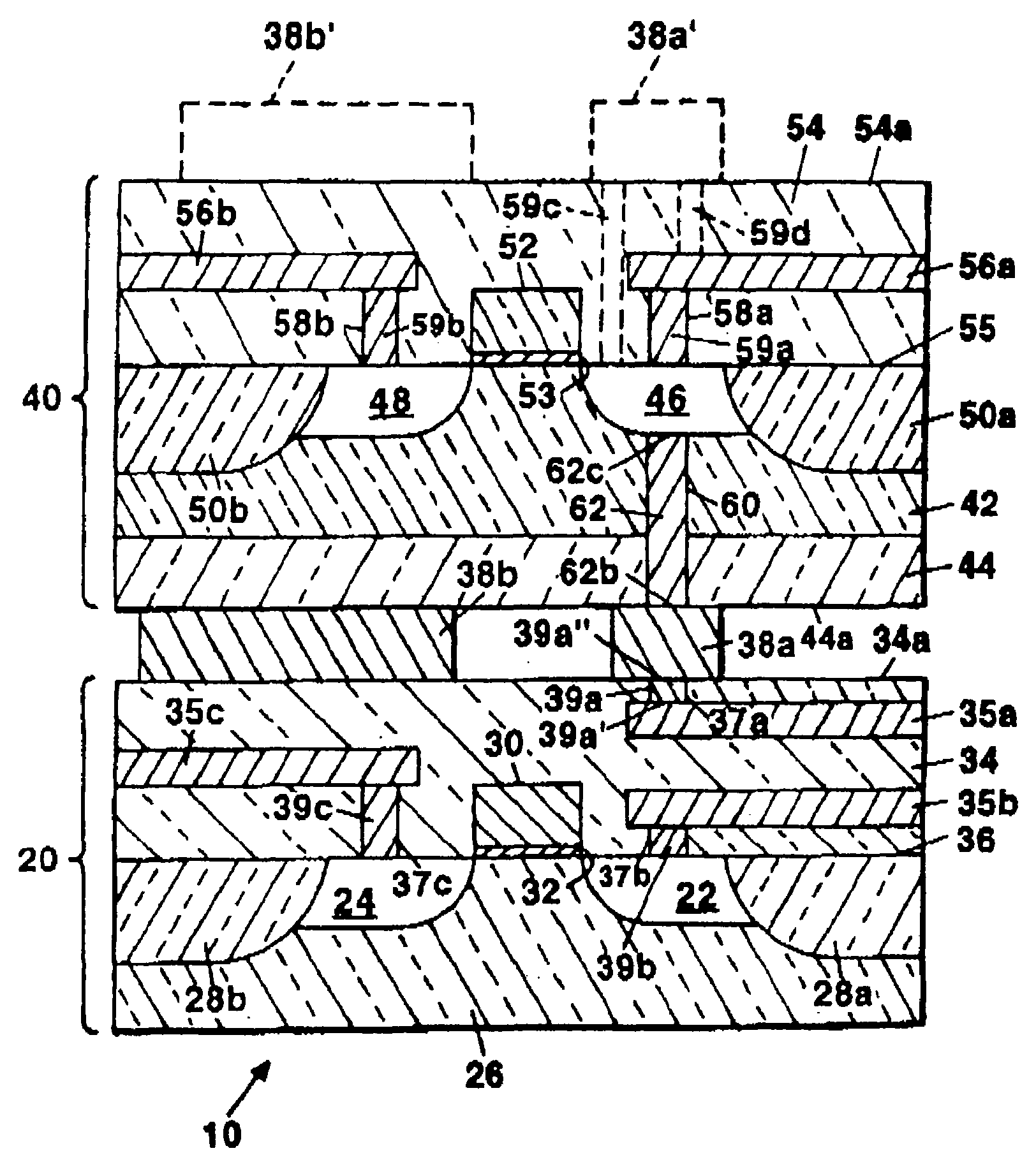
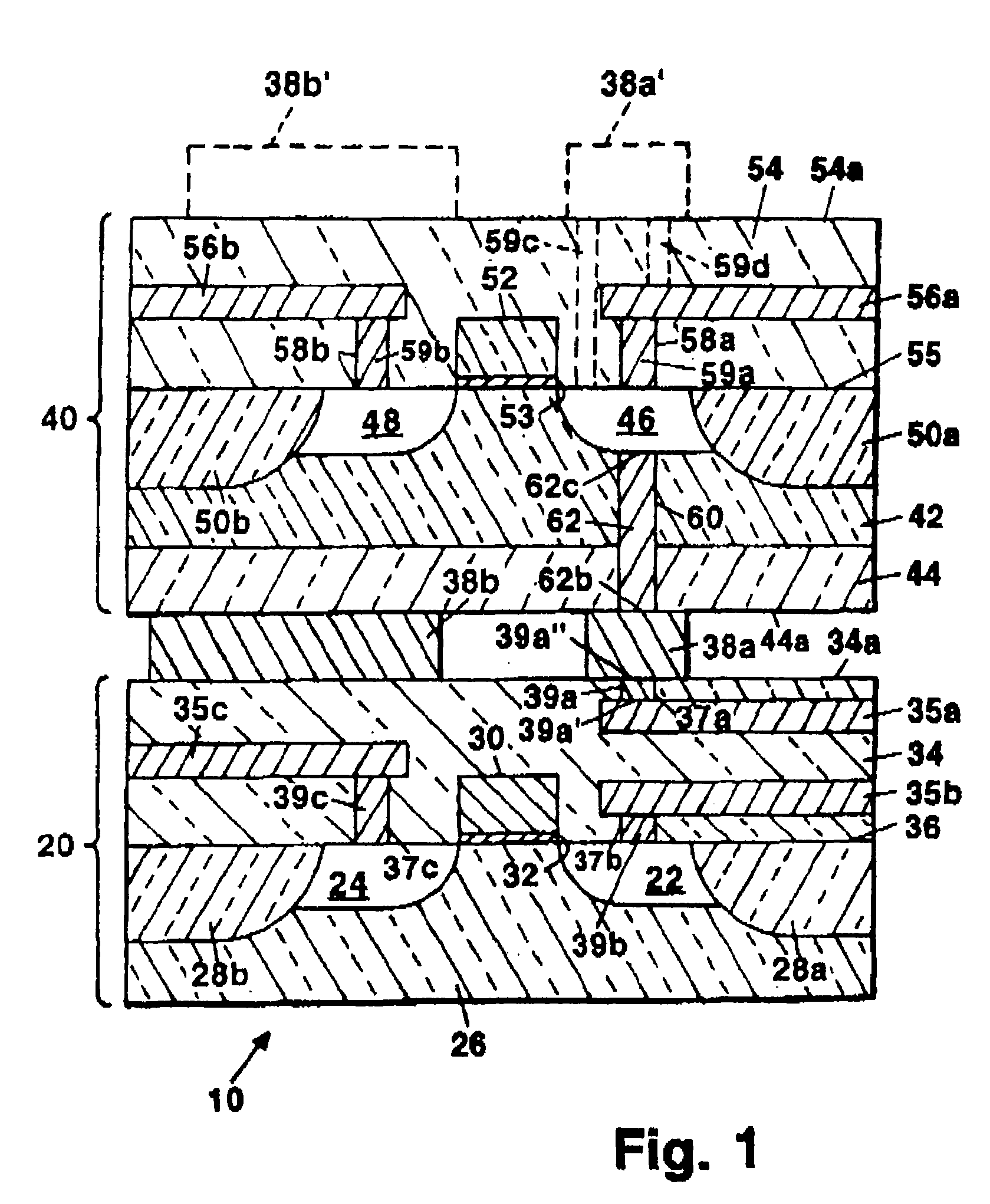
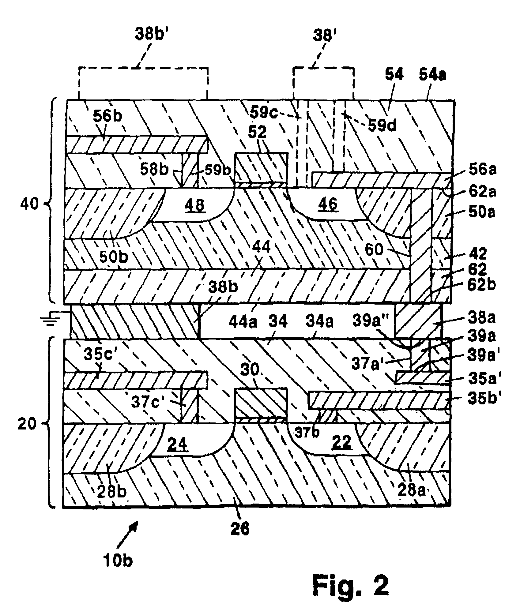
[0021]Referring to FIG. 1, a multi-layer integrated semiconductor structure 10 includes at least a first device layer 20 and a second device layer 40. The first and second device layers (20 and 40 respectively) represent separate semiconductor device structures, each of which may include a number of layers. For example, the first device layer 20 may correspond to a first semiconductor wafer consisting of several semiconductor devices and metal interconnect layers while the second device layer 40 corresponds to a second semiconductor wafer consisting of several semiconductor devices and metal interconnect layers. In addition, device layers 20, 40 may also represent individual dies cut from a wafer. The first and second device layers 20, 40 are bonded together by first and second interface portions 38a, 38b. In one embodiment, the first interface portion 38a is employed for electrically connecting the first and second device layers 20, 40, while the second interface portion 38b is emp...


PUM


Abstract

A multi-layer integrated semiconductor structure is provided, which includes at least a first semiconductor structure and a second semiconductor structure coupled together via an interface. The interface includes at least a first portion adapted to provide a communication interface between the first semiconductor structure and the second semiconductor structure and at least a second portion adapted to reduce electrical interference between the first semiconductor structure and the second semiconductor structure.

Description

CROSS REFERENCE TO RELATED APPLICATION[0001]This application claims the benefit under 35 U.S.C. §119(e) of U.S. Provisional Application No. 60 / 437,549, filed on Dec. 31, 2002, entitled, A Multi-Layer Integrated Semiconductor Structure, which is hereby incorporated by reference in its entirety.STATEMENT REGARDING FEDERALLY SPONSORED RESEARCH[0002]This invention was made with government support under a subcontract between Georgia Institute of Technology and M.I.T., under Prime Grant Number MDA972-99-1-0002, awarded by the Defense Advanced Research Projects Agency. The government has certain rights in the invention.FIELD OF THE INVENTION[0003]The present invention relates generally to a multi-layer integrated semiconductor structure and, more specifically, to a multi-layer integrated semiconductor structure that includes one or more electrical interference shielding portions. The purpose of such structures is to electrically isolate active devices fabricated in one semiconductor layer ...

Claims


Application Information

Patent Timeline
Patent Type & Authority Patents(United States)
IPC IPC(8): H01L23/02H01L21/60H01L21/68H01L23/48H01L23/522H01L25/065
CPCH01L21/6835H01L23/481H01L23/5226H01L24/81H01L25/0657H01L24/05H01L2924/0002H01L2924/1306H01L2924/1461H01L2924/01075H01L2924/01072H01L23/522H01L2221/68359H01L2224/0557H01L2224/81801H01L2224/81894H01L2224/8383H01L2225/06513H01L2225/06527H01L2225/06541H01L2225/06596H01L2924/01005H01L2924/01006H01L2924/01007H01L2924/01013H01L2924/01014H01L2924/01015H01L2924/01016H01L2924/01025H01L2924/01029H01L2924/0104H01L2924/01054H01L2924/01057H01L2924/01061H01L2924/01073H01L2924/01074H01L2924/01079H01L2924/05042H01L2924/12044H01L2924/14H01L2924/19041H01L2924/19042H01L2924/19043H01L2924/30105H01L2924/3025H01L2924/01019H01L2924/01033H01L2924/00H01L2224/05552H01L2924/00011H01L2924/12042H01L2224/0401H01L2224/83205
Inventor REIF, RAFAELCHECKA, NISHACHANDRAKASAN, ANANTHA
Owner MASSACHUSETTS INST OF TECH
Why Eureka
Try Eureka