Plasma display device and driving method thereof
a technology of a display device and a driving method, which is applied in the direction of instruments, television systems, and electrodes, etc., can solve the problems of reducing the resolution of the screen, short life of fluorescent materials, and prone to impact of fluorescent materials
- Summary
- Abstract
- Description
- Claims
- Application Information
AI Technical Summary
Benefits of technology
Problems solved by technology
Method used
Image
Examples
first embodiment
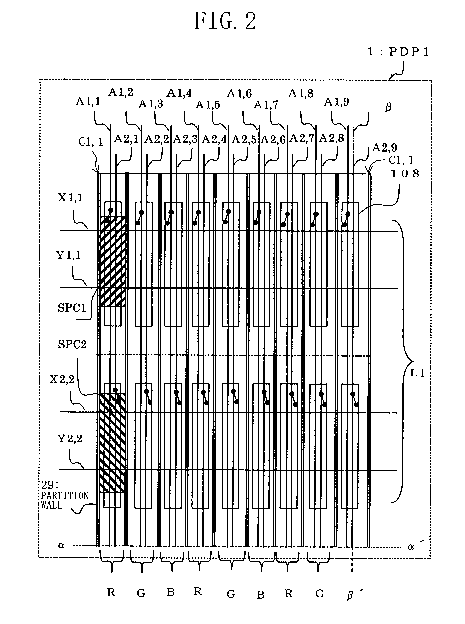
[0160]In the plasma display device of the first embodiment, each pixel is formed by a plurality of sub pixels of the same color provided in the address-electrode direction. This plasma display device provides gray-scale display by controlling the number of sub pixels to be turned ON. In this plasma display device, a plurality of address electrodes are provided for each sub pixel, and each sub pixel is addressed by a second conductive layer 108 which is electrically connected to one of the plurality of address electrodes. The plasma display device of the first embodiment thus provides a solution to implement a greater number of gray levels and higher definition.
[0161]The structure of the first embodiment will now be described with reference to FIG. 2.
[0162]FIG. 2 is an enlarged partial schematic plan view showing the region of sub pixels SPC1, SPC2 of pixels C1,1 to C9,1 in the PDP 1.
[0163]Each pixel CM,N of the PDP 1 is formed by two sub pixels provided in the address-electrode dire...
second embodiment
[0177]In the plasma display device of the second embodiment, each pixel is formed by a plurality of sub pixels of the same color provided in the X-electrode direction. This plasma display device provides gray-scale display by controlling the number of sub pixels to be turned ON. In this plasma display device, a plurality of address electrodes are provided for each sub pixel, and each sub pixel is addressed by a second conductive layer which is electrically connected to one of the plurality of address electrodes. The plasma display device of the second embodiment thus provides a solution to implement a greater number of gray levels and higher definition.
[0178]The structure of the second embodiment will now be described with reference to FIG. 4.
[0179]FIG. 4 is an enlarged partial schematic plan view showing the region of pixels C1,1 to C5,2 in the PDP 1.
[0180]Each unit pixel CM,N of the PDP 1 is formed by two sub pixels provided in the X-electrode direction (where M is in the range of...
third embodiment
[0194]The plasma display device of the third embodiment includes a plurality of sub pixels provided adjacent to each other. The plurality of sub pixels include two types of sub pixels having different electrode lengths in the direction in which the plurality of sub pixels are arranged. In other words, in the two types of sub pixels, an electrode extends with different lengths in the direction in which the plurality of sub pixels are arranged. The plasma display device of the third embodiment provides gray-scale display by controlling a combination of sub pixels to be turned ON, thereby providing a solution to implement a greater number of gray levels and higher definition.
[0195]The structure of the third embodiment will now be described with reference to FIG. 5.
[0196]FIG. 5 is an enlarged partial schematic plan view showing the region of pixels C1,1 to C3,2 in the PDP 1.
[0197]Each pixel CM,N of the PDP 1 is formed by two sub pixels provided in the row direction (where M is in the ra...
PUM
 Abstract
Description
Claims
Application Information


