Inspecting method, inspecting system, and method for manufacturing electronic devices

a technology of electronic devices and inspection methods, applied in image enhancement, instruments, image data processing, etc., can solve the problems of insufficient consideration of the user interface (image display) used in the classifying operation, requiring an extensive time for the classifying operation, and the analysis accuracy also tends to be too low, so as to shorten the analysis time, enhance the analysis accuracy, and improve the effect of user interfa

Inactive Publication Date: 2006-06-27
HITACHI LTD
View PDF11 Cites 34 Cited by
  • Summary
  • Abstract
  • Description
  • Claims
  • Application Information

AI Technical Summary

Benefits of technology

[0005]It is an object of the present invention to shorten the analysis time and enhance the analysis accuracy by improving the user interface. It is a further object of the present invention to enhance the yield of the production line.

Problems solved by technology

However, the user interface (image display) used in the classifying operation has not been sufficiently considered.
Therefore, with the conventional system, it is difficult to efficiently classify a number of detected images, thereby not only requiring an extensive time for the classifying operation, but the analysis accuracy also tends to be too low.
Further, there is a possibility that the retirement of long time periods for the classifying operation will result in a delay in a feedback operation and a great hindrance to the yield of the production line.

Method used


Image

  • Inspecting method, inspecting system, and method for manufacturing electronic devices
  • Inspecting method, inspecting system, and method for manufacturing electronic devices
  • Inspecting method, inspecting system, and method for manufacturing electronic devices

Examples


Embodiment Construction

[0025]Embodiments of the present invention will now be described in detail with reference to the accompanying drawings.

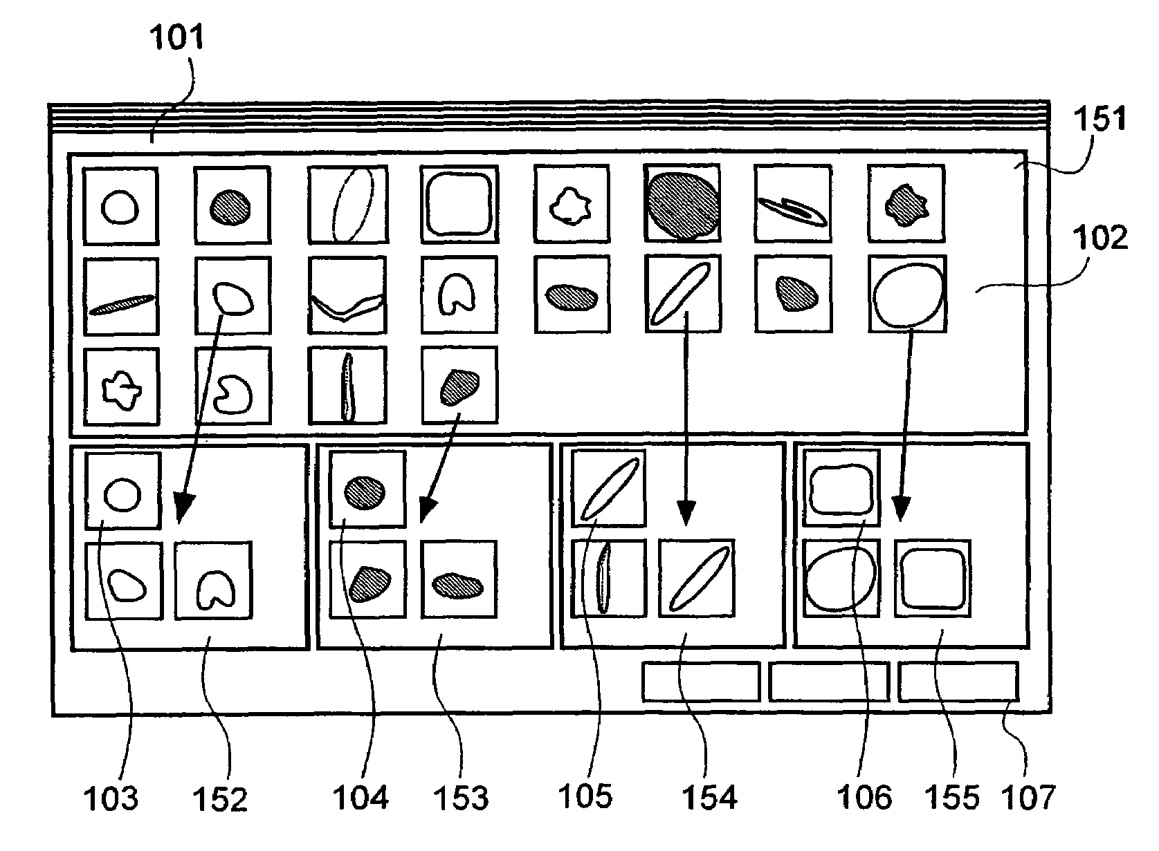
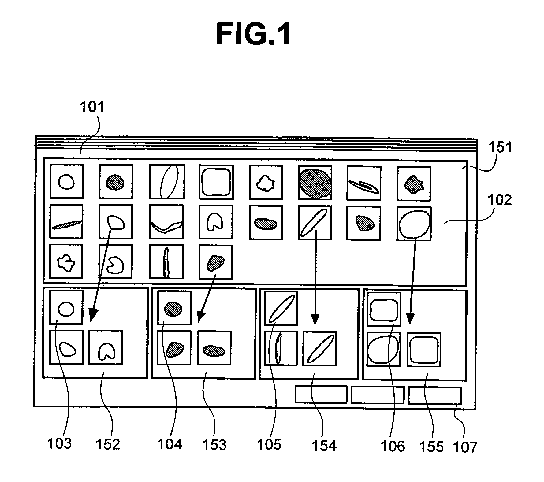
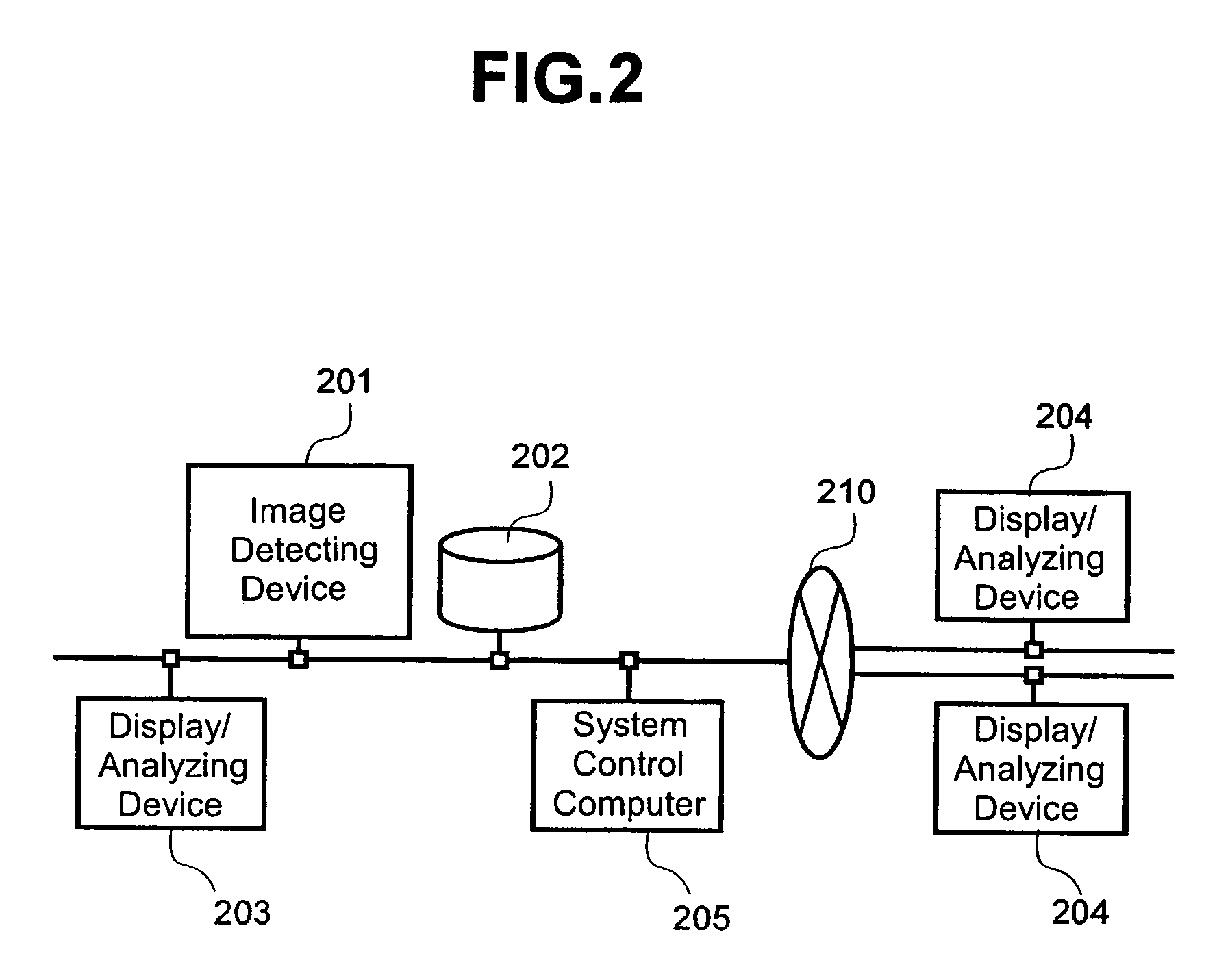
[0026]FIG. 1 is a view showing an example of a display illustrating a classification function performed on detected defect images on a PC (Personal Computer) display screen equipped with an analyzing unit. In the figure, reference numeral 101 designates a display screen of a PC. Numeral 151 designates an unclassified image display area for displaying detected defect images which have not been subjected to a classification operation. Numeral 102 designates detected individual defect images displayed in the unclassified image display area 151. Numerals 152 to 155 designate classification areas for classifying defect images. Numerals 103 to 106 designate typical defect images having features assigned to the classification areas 152 to 155, respectively. For example, a typical defect image 103 having a white and round defect feature is displayed in area 152, a typical b...


PUM

PropertyMeasurementUnit
areaaaaaaaaaaa
defect classificationaaaaaaaaaa
defectaaaaaaaaaa

Abstract

The present invention has an analyzing unit including an image detection device for producing a plurality of images of a workpiece, a storage for storing detected images produced by the image detection device, and a display having a screen with a first area for displaying a plurality of detected images stored in the storage and a plurality of second areas for classifying the detected images according to features of the detected images, whereby the plurality of detected images are moved on the screen from the first area to selected second areas to classify the plurality of detected images in the second areas.

Description

BACKGROUND OF THE INVENTION[0001]The present invention relates to an analyzing unit, an inspecting system and a manufacturing method using the inspecting system, which are applied to a production line used in the manufacture of electronic devices and the like; and, more particularly, the invention relates to an analyzing unit, an inspecting system and a manufacturing method using the inspecting system, which efficiently classify images obtained as a result of inspection of devices being manufactured, to thereby shorten the analysis time required to detect a failure on the production line and to enable enhancement of manufacturing efficiency and a rapid yield ramp-up.[0002]An electronic device, typically a semiconductor, is formed by repeating a plurality of processing steps, including exposure, development, etching and the like, on a wafer substrate. On the other hand, in certain ones of the plurality of processing steps, information indicating the position, size, number, category, ...

Claims


Application Information

Patent Timeline
Patent Type & Authority Patents(United States)
IPC IPC(8): G06K9/00G01N21/84G06F3/00G06F3/048G06F3/0486G06T1/00G06T7/00
CPCG06F3/0486G06T7/0004G06F2203/04803G06T2207/30148G06T2200/24
Inventor IKEDA, YOKOKONISHI, JUNKOIWATA, HISAFUMITAKAGI, YUJIOBARA, KENJINAKAGAKI, RYOISOGAI, SEIJIOZAWA, YASUHIKO
Owner HITACHI LTD
Why Eureka
Try Eureka