Array structure of two-transistor cells with merged floating gates for byte erase and re-write if disturbed algorithm

a transistor cell and floating gate technology, applied in static storage, digital storage, instruments, etc., can solve the problems of increasing the amount of semiconductor real estate required to implement byte alterable memory, and cost sensitive, so as to reduce the amount of byte alterable memory, and prevent punching

Inactive Publication Date: 2006-07-04
TAIWAN SEMICON MFG CO LTD
View PDF13 Cites 26 Cited by
  • Summary
  • Abstract
  • Description
  • Claims
  • Application Information

AI Technical Summary

Benefits of technology

[0012]It is another objective of the present invention to eliminate punch-through disturb and reverse tunnel disturb conditions in a split gate memory array.
[0021]The need to have a separate source lines for odd and even addressed cells is eliminated by a cell that is connected to a program bit line and a read bit line. The two bit lines connect to two separate split gate transistors (a program transistor and a read transistor) in which the floating gate is shared between the two transistors by merging the floating gate for the program transistor with the floating gate of the read transistor. Punch-through disturb is eliminated in cells containing the two transistors with merged floating gates which are connected to a common source line because the cells are arranged such that there is not a common program bit line for cells with a common source line. Applying approximately 1.8V on the unselected word line eliminates reverse tunneling.
[0022]In another embodiment of the present invention the program transistor of a merged floating gate two transistor pair has an added implant to raise the Vt of the program transistor. This added implant increases the Vt (threshold voltage) of the program transistor and prevents punch through on the program transistor. Since the program transistor is not used for reading, the cell current can be small allowing the higher Vt. The word line voltage may need to be raised and as a result the difference between word line inhibit voltage and word line read voltage is increased.

Problems solved by technology

These applications are cost sensitive and require that the byte alterable capability be implemented at a minimum cost.
Creating a byte alterable memory, in general, requires segmentation of word lines and source lines, which in turn adds to the amount of semiconductor real estate required to implement the byte alterable memory.

Method used


Image

  • Array structure of two-transistor cells with merged floating gates for byte erase and re-write if disturbed algorithm
  • Array structure of two-transistor cells with merged floating gates for byte erase and re-write if disturbed algorithm
  • Array structure of two-transistor cells with merged floating gates for byte erase and re-write if disturbed algorithm

Examples


first embodiment

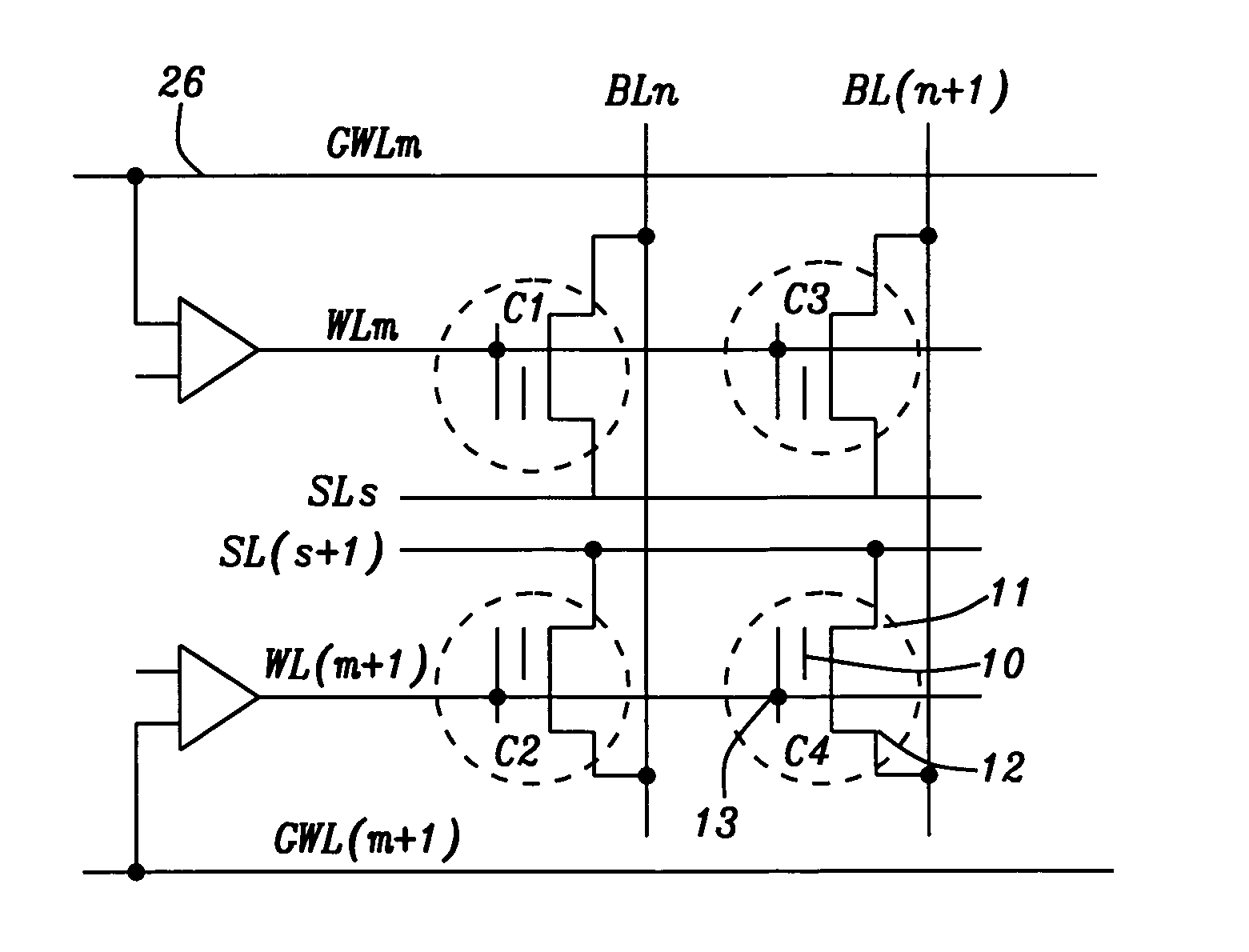
[0036]In FIG. 2 is shown a portion of a memory array of the present invention containing cells C1, C2, C3, and C4 with a single split gate transistor. The control gates 13 of the odd designated cells C1 and C3 are coupled to a local word line WLm and the control gates 13 of the even designated cells C2 and C4 are coupled to a local word line WL(m+1). The local word lines WLm and WL(m+1) are driven by word line drivers 25 which are connected to global word lines GWLm and GWL(m+1). The global word line 26 can be effectively segmented into small segments such as a byte length using a plurality of word line drivers 25 along a row of memory cells to drive each segment of cells. The source line connecting the odd cells and the even cells are separated into a source line SLs coupled to cells C1 and C3 and source line SL(s+1) coupled to cells C2 and C4. If cell C3 is selected to be programmed, The selected local word line WLm voltage is at approximately +1.8V, the voltage of unselected word...

second embodiment

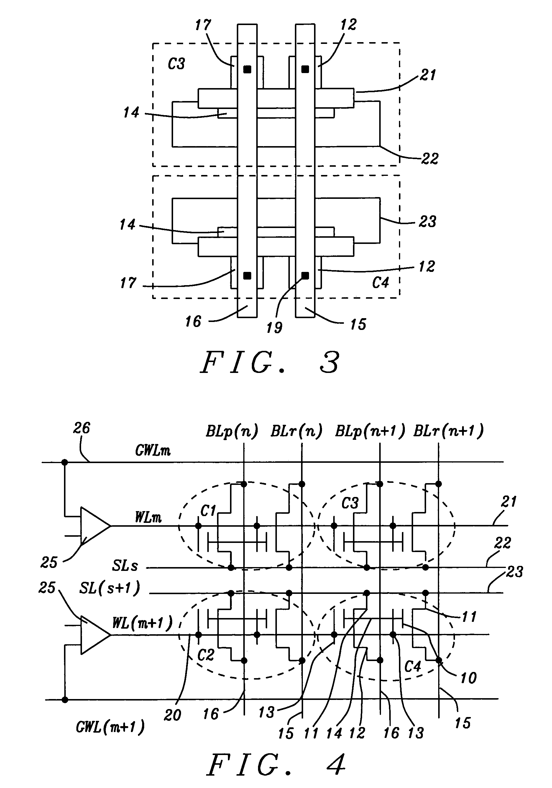
[0037]the present invention is described with respect to FIG. 3 and FIG. 4. FIG. 3 shows the plan view of the layout of two vertically adjacent cells C3 and C4. FIG. 4 shows a schematic diagram of a portion of an array of nonvolatile cells C1, C2, C3 and C4. The reference numbers in FIG. 3 and FIG. 4 correspond to each other and will be used to describe the layout and interconnections of the cells.

[0038]Continuing to reference FIGS. 3 and 4, each cell C1, C2, C3 and C4 comprise two split gate transistors that are coupled together by a shared, or merged, floating gate 14. Two bit lines 15 and 16 connect between cells in a column, which are connected to the drains 12 of the transistors by contacts 19. Cells C1 and C2 are connected by bit lines BLp(n) 16, a program bit line, and BLr(n)15, a read bit line. Cells C3 and C4 are connected by bit lines BLp(n+1) 16, a program bit line, and BLr(n+1) 15, a read bit line. A word line WLm 21 connects to the control gates 13 in a row of cells con...

third embodiment

[0039]A third embodiment is shown in FIG. 5A in which there are two three-transistor cells C3 and C4 oriented one above the other in a column. The corresponding schematic diagram is shown in FIG. 6. There are three bit lines, two program bit lines 31 and 33 and one read bit line 32. In FIG. 6 the program bit lines are designated as BLp0(n) 34, BLp1(n) 36, BLp0(n+1) 31 and BLp1(n+1) 33, and the read bit lines are designated as Blr(n) 35 and BLr(n+1) 32. Each cell C1, C2, C3 and C4 contain two split gate transistors, which have a merged floating gate 37. The third transistor in each cell is a split gate transistor separate from the other two and having a self-contained floating gate 38. The third transistor provides a “dummy” function that distributes capacitive loading on the program bit lines. Cells C3 and C4 are reversed mirror images of each other such that the “dummy” transistor is located at the upper right and lower left in FIG. 5A, and identified by the floating gate 38. The c...


PUM


Abstract

Variations in memory array and cell configuration are shown, which eliminate punch-through disturb, reverse-tunnel. Several configurations are shown which range from combined and separate source lines for each row of cells, a two transistor cell containing a read transistor and a program transistor connected by a merged floating gate, and a two transistor cell where the program transistor has an extra implant to raise the Vt of the transistor to protect against punch-through disturb. A method is also described to rewrite disturbed cells, which were not selected to be programmed.

Description

BACKGROUND OF THE INVENTION[0001]1. Field of Invention[0002]The present invention relates to semiconductor memory and in particular to an array structure using split gate transistor cells and providing ways to avoid reverse-tunnel-disturb and punch through-disturb as well as a method to re-write cells that are feed forward disturbed.[0003]2. Description of Related Art[0004]Applications such as data memory or smart card require a byte alterable memory. These applications are cost sensitive and require that the byte alterable capability be implemented at a minimum cost. In order to keep a byte alterable memory compact, an array architecture is required that provides a compact memory and eliminates any resulting disturb conditions. Creating a byte alterable memory, in general, requires segmentation of word lines and source lines, which in turn adds to the amount of semiconductor real estate required to implement the byte alterable memory.[0005]U.S. Pat. No. 6,376,876 B1 (Shin et al.) i...

Claims


Application Information

Patent Timeline
Patent Type & Authority Patents(United States)
IPC IPC(8): G11C16/04G11C11/34G11C16/34
CPCG11C16/0425G11C16/3427G11C16/3418
Inventor CHIH, YEU-DER
Owner TAIWAN SEMICON MFG CO LTD
Why Eureka
Try Eureka