Semiconductor memory device and refresh control method

a memory device and memory technology, applied in the field of semiconductor memory devices, can solve the problems of increasing the cost of device testing to the total chip cost, the failure of digit-disturb-hold tests, and the long test time of failures, so as to improve the data-hold characteristics of memory cells, reduce test time, and increase the speed of access time

Inactive Publication Date: 2008-04-22
RENESAS ELECTRONICS CORP
View PDF9 Cites 8 Cited by
  • Summary
  • Abstract
  • Description
  • Claims
  • Application Information

AI Technical Summary

Benefits of technology

[0020]As a result, test time of the semiconductor-memory device by an test equipment, and especially test time of a digit (bit)-disturb-hold test that verifies whether there is data hold time, increases, and hence the ratio of the cost for device testing to the total chip cost increases. The reason for that is as follows. In the digit-disturb-hold test, data is written to all of the memory cells in which the gates of the MOS transistors (cell transistors) are connected to the word lines other than the specified word line for which disturbance is performed, and while the target cell holds data, by setting the number of times the word lines are to be alternated between selection level and non-selection level, the effect on the memory data held in the target cell is checked. For example, when the data hold characteristic of a memory cell is 16 ms and the access time (clock cycle) is 100 ns, in order to satisfy such a standard that assumes a data hold time of 16 ms, the number of accesses becomes 1.6 million times. In the case of a memory cell whose data-hold characteristic is not good, charge stored in a cell capacitor leaks through the MOS transistor. This digit-disturb-hold test requires a failure long test time. Particularly, in the case of a semiconductor-memory device that performs refresh during a standby state, and performs hidden refresh in an active state, the refresh operation is performed by control inside the semiconductor-memory device, which is independent of control by a memory tester, and when the aforementioned delay occurs, the test time of the digit-disturb-hold test becomes further longer.
[0031]With the present invention, in the active state, it is possible to set the timer period that regulates the refresh period to a short period, and together with being able to reduce the test time, it is possible to improve the data-hold characteristics of the memory cells. With this invention, restrictions of the disturb conditions in the active state that are critical to the standards for the refresh period (data hold time) are done away with.
[0032]Furthermore, with the present invention, since refresh is not performed when changing from the standby state to the active state, delays in read / write access do not occur when changing to the active state, making it possible to increase the speed of the access time.

Problems solved by technology

In the conventional semiconductor-memory device described referring to FIG. 5 and FIG. 6, in the standby mode particularly, self refresh is performed entirely based on a timeout of the timer 8 provided in the semiconductor-memory device, and read / write access supplied from the outside is performed asynchronously, so to speak, so it is difficult to adequately control the occurrence of the aforementioned delay.
As a result, test time of the semiconductor-memory device by an test equipment, and especially test time of a digit (bit)-disturb-hold test that verifies whether there is data hold time, increases, and hence the ratio of the cost for device testing to the total chip cost increases.
This digit-disturb-hold test requires a failure long test time.

Method used


Image

  • Semiconductor memory device and refresh control method
  • Semiconductor memory device and refresh control method
  • Semiconductor memory device and refresh control method

Examples


Embodiment Construction

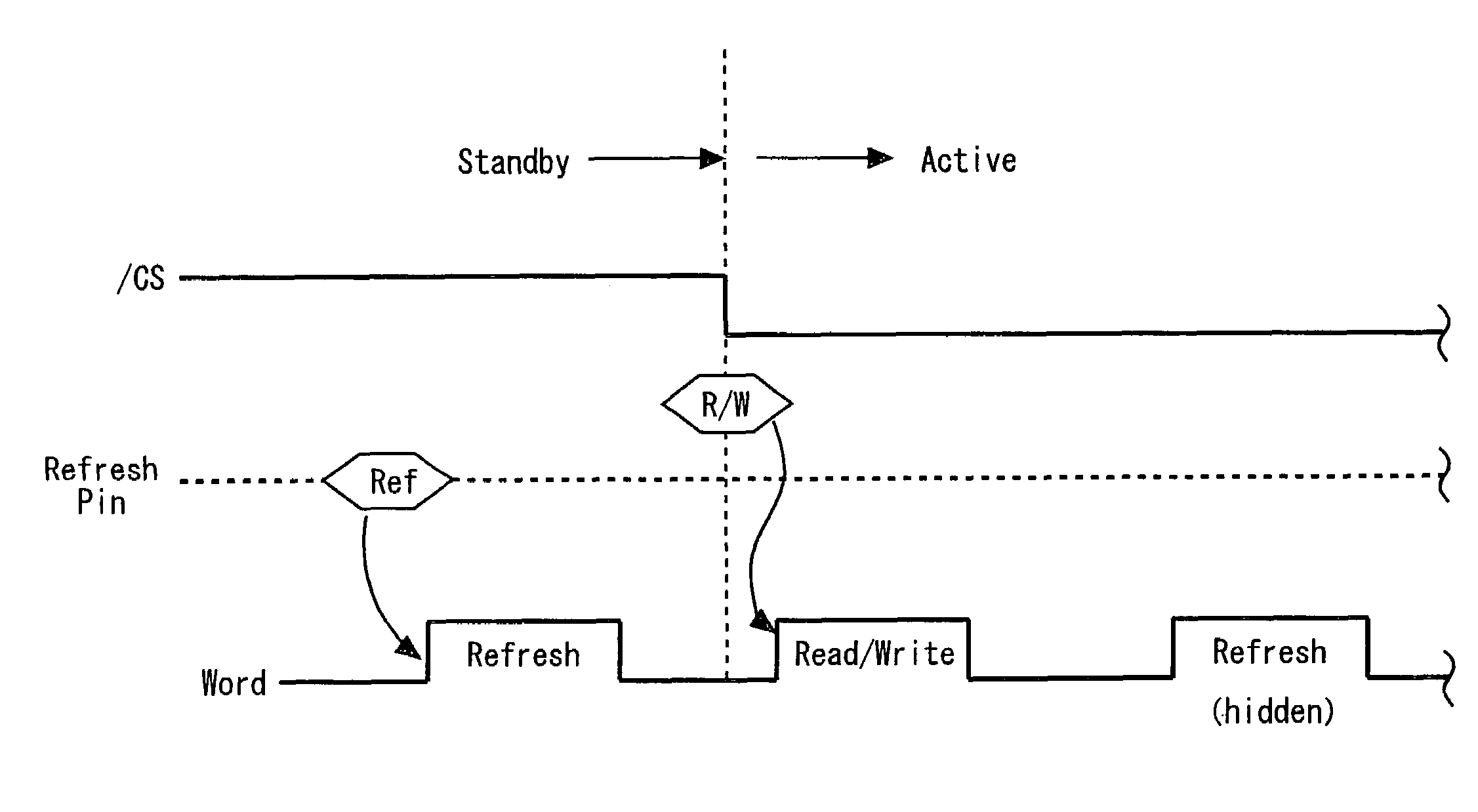
[0040]A preferred embodiment of the invention will be described below with reference to accompanying drawings. With a semiconductor-memory device according to the present invention, a refresh-execution command is supplied to the semiconductor-memory device from the outside by a CPU, controller and the like, in a standby state. The semiconductor-memory device receives the refresh-execution command and performs the refresh operation. In an active state, the semiconductor-memory device performs hidden refresh that hides the refresh operation from the outside. Any method can be used for performing hidden refresh.

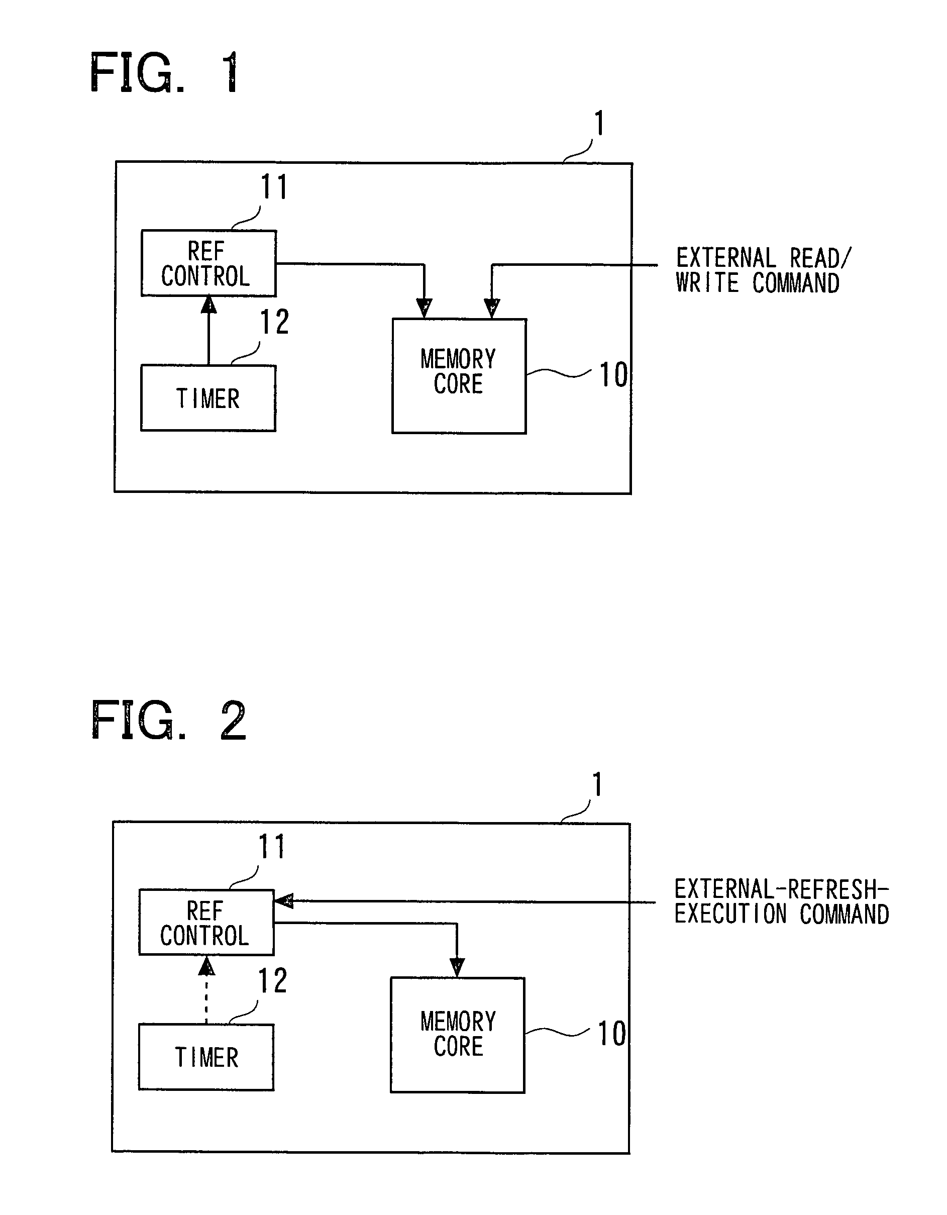
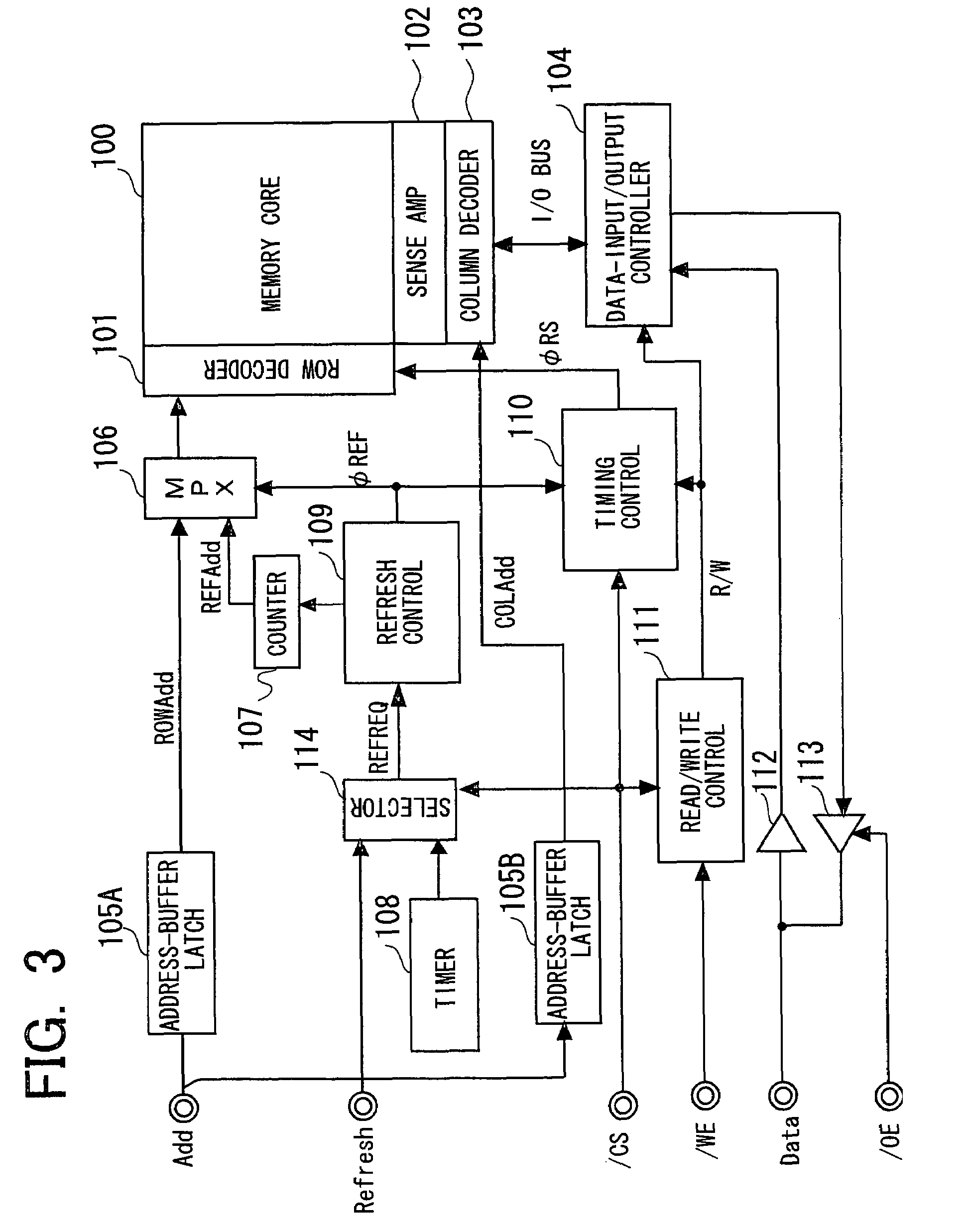
[0041]FIG. 1 is a diagram showing the configuration of an embodiment of the present invention. In FIG. 1, the configuration of a semiconductor-memory device in an active state is schematically illustrated. Referring to FIG. 1, when a semiconductor-memory device 1 is in the active state, an external read / write command supplied to the semiconductor-memory device 1 from outside the...


PUM


Abstract

Disclosed is a semiconductor-memory device comprising a selector for performing switching control such that in the standby state the refresh operation is performed responsive to an external-refresh-execution command supplied from outside the semiconductor-memory device, while in the active state, the refresh operation is performed, not under the control from outside the semiconductor-memory device, but under the control from a built-in timer.

Description

FIELD OF THE INVENTION[0001]This invention relates to a semiconductor-memory device, and more particularly to a semiconductor-memory device that requires refreshing so that data is retained and a refresh control method thereofBACKGROUND OF THE INVENTION[0002]A dynamic-type semiconductor-memory device (DRAM) comprises a plurality of memory cells, each of which has one transistor and one capacitor, and which occupies a small area. In a DRAM, information is recorded by storing data in the capacitor, so due to leak current, charge stored in the memory cell decreases over time. Therefore, before the stored information is lost, it is necessary to perform a refresh operation in which the information stored in a memory cell is read by a sense amplifier, and then the read data is restored to the memory cell by that sense amplifier. On the other hand, a static-type semiconductor-memory device (SRAM) comprises a plurality of memory cells, each of which is composed by a flip-flop. In a SRAM, a ...

Claims


Application Information

Patent Timeline
Patent Type & Authority Patents(United States)
IPC IPC(8): G11C7/00
CPCG11C11/406G11C11/40615G11C2211/4061
Inventor TAKAHASHI, HIROYUKI
Owner RENESAS ELECTRONICS CORP
Why Eureka
Try Eureka