
Structure for an LDMOS transistor and fabrication method for thereof

a technology of ldmos transistor and structure, which is applied in the direction of semiconductor devices, electrical equipment, basic electric elements, etc., can solve the problems of inability to precisely control the overlap width of gate layers, the effective channel length l/sub>d/sub>being too long, and the gate layer b>24/b> may shift, etc., to achieve the effect of effective channel length

Inactive Publication Date: 2006-07-11
VANGUARD INTERNATIONAL SEMICONDUCTOR CORPORATION
View PDF2 Cites 3 Cited by
  • Summary
  • Abstract
  • Description
  • Claims
  • Application Information

AI Technical Summary

Benefits of technology

The present invention provides an LDMOS transistor with a horseshoe-shaped gate layer and a pair of P bodies to precisely control an overlapping width between the gate layer and the P body, thus ensuring the effective channel length of the LDMOS transistor. This structure allows for better control over the transistor's performance and reliability.

Problems solved by technology

However, the limitations in small-size design and thermal budget always cause the overlapping portion to shift, resulting in the effective channel length LD being to long or too short.
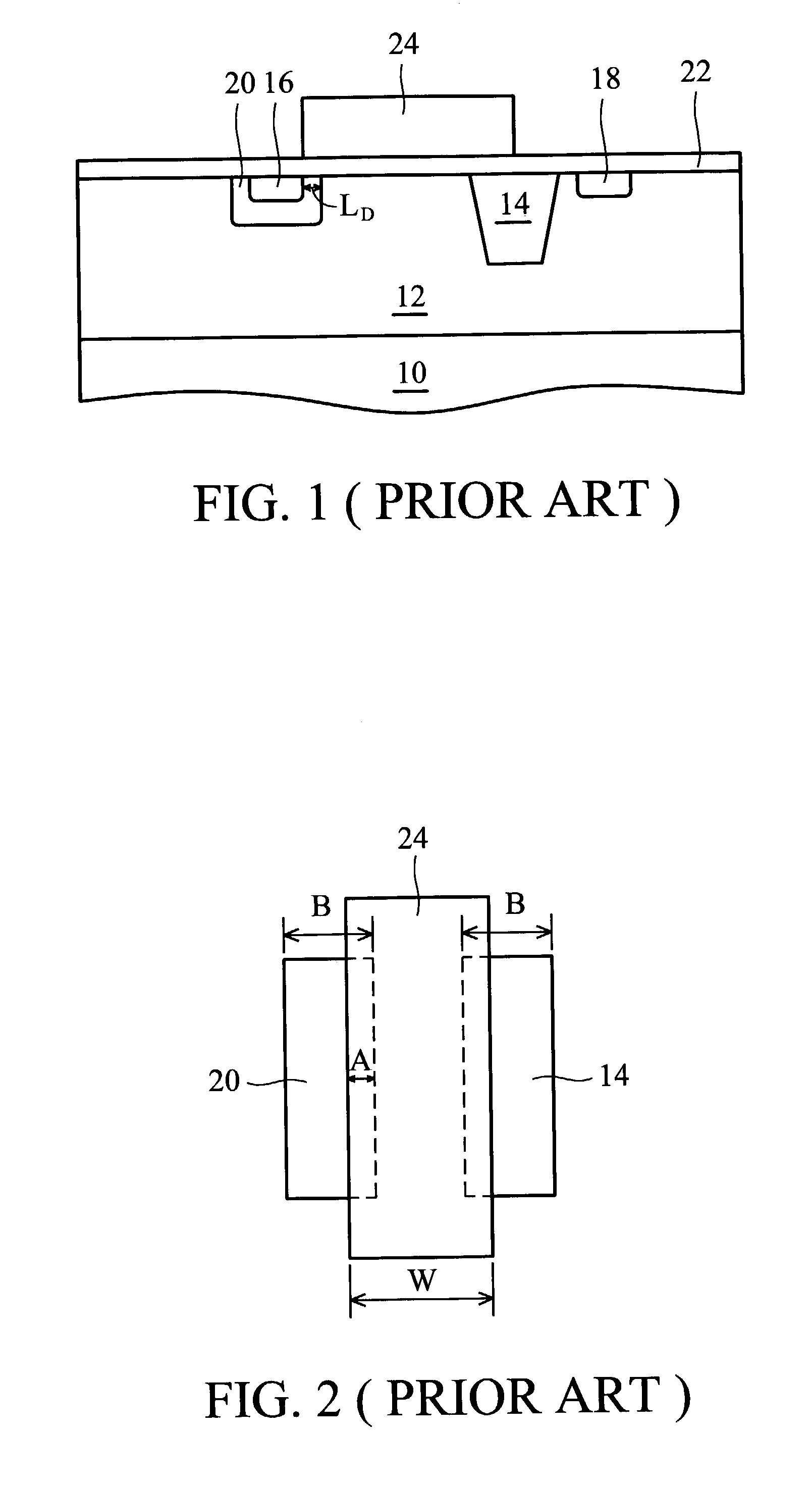
Nevertheless, due to the exposure limitation, the gate layer 24 may shift and fail to precisely control the overlapping width A.

Method used


Image

  • Structure for an LDMOS transistor and fabrication method for thereof
  • Structure for an LDMOS transistor and fabrication method for thereof
  • Structure for an LDMOS transistor and fabrication method for thereof

Examples


Embodiment Construction

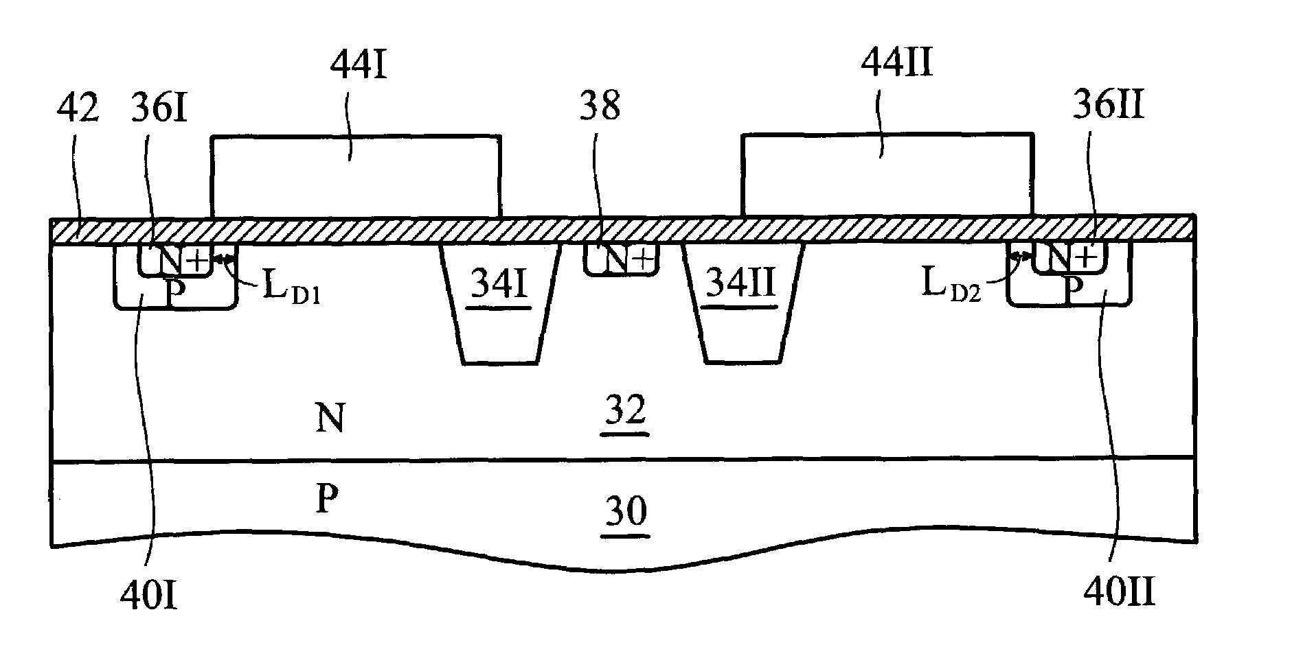
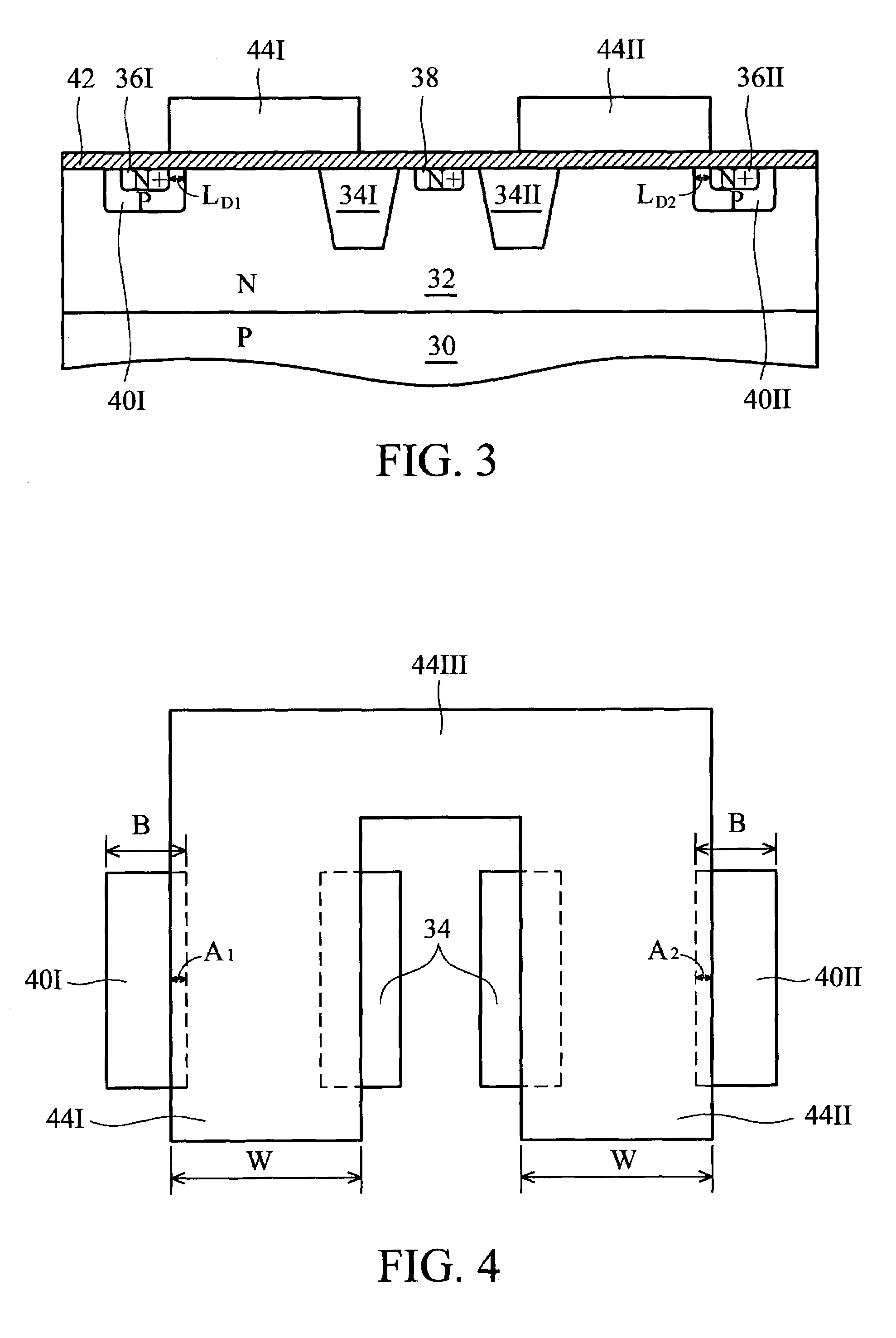
[0016]FIG. 3 is a sectional diagram of an LDMOS transistor of the present invention. FIG. 4 is a plane view of a gate layer and P bodies of the present invention.

[0017]In a case of a high-voltage area of a P-type semiconductor silicon substrate 30, an N-type silicon layer 32 is provided thereon, and a first STI structure 34I and a second STI structure 34II are formed in the N-type silicon layer 32 to isolate components within the high-voltage area. The N-type silicon layer 32 may be an N-type epitaxial layer or an N-type well layer. Also, the N-type silicon layer 32 comprises a first N+-type source region 36I at a left side of the first STI structure 34I, a second N+-type source region 36II at a right side of the second STI structure 34II, a N+-type drain region 38 between the first STI structure 34I and the second STI structure 34II. Moreover, the N-type silicon layer 32 comprises a first P body 40I surrounding the sidewalls and bottom of the first N+-type source region 36I, and a ...


PUM


Abstract

A structure for an LDMOS transistor has a horseshoe-shaped gate layer formed on a N-type layer of a semiconductor silicon substrate, in which the gate layer comprises a transverse-extending area, a first lengthwise-extending area connected to a left end of the transverse-extending area and a second lengthwise-extending area connected to a right end of the transverse-extending area. A first P-type body is formed in the N-type layer, and overlaps the left periphery of the first lengthwise-extending area of the gate layer. A second P-type body is formed in the N-type layer, and overlaps the right periphery of the second lengthwise-extending area of the gate layer.

Description

BACKGROUND OF THE INVENTION[0001]1. Field of the Invention[0002]The invention relates to a high-voltage power device, and more particularly to a gate layer and a P body used for an LDMOS transistor.[0003]2. Description of the Related Art[0004]Recently, as the manufacturing techniques of semiconductor integrated circuits have developed, to fulfill requests for the integration of controllers, memories, low-voltage operating circuits and high-voltage power devices on a single chip, to achieve a single-chip system, in which a power device, including vertical diffused MOS (VDMOS) transistor, lateral diffused MOS (LDMOS) transistor and insulated gate bipolar transistor (IGBT), is used to increase power transforming efficiency and decrease wasted energy. The LDMOS transistor compatible with the high-voltage CMOS process is prevalent in the manufacture of high-voltage power devices.[0005]FIG. 1 is a sectional diagram of a conventional LDMOS transistor. In a case of a high-voltage area of a ...

Claims


Application Information

Patent Timeline
Patent Type & Authority Patents(United States)
IPC IPC(8): H01L21/336H01L21/8234H01L29/06H01L29/423H01L29/78
CPCH01L29/7801H01L29/0653H01L29/4238H01L29/7816
Inventor YANG, JIA-WEICHANG, DA-PONGLIAO, CHIH-CHERNG
Owner VANGUARD INTERNATIONAL SEMICONDUCTOR CORPORATION
Learn More