

Manufacturing method of metal oxide semiconductor field effect transistor
A technology of oxide semiconductors and field effect transistors, which is applied in semiconductor/solid-state device manufacturing, electrical components, circuits, etc., and can solve problems that affect device performance and design size shortening
- Summary
- Abstract
- Description
- Claims
- Application Information
AI Technical Summary
Problems solved by technology
Method used
Image

Examples
Embodiment approach
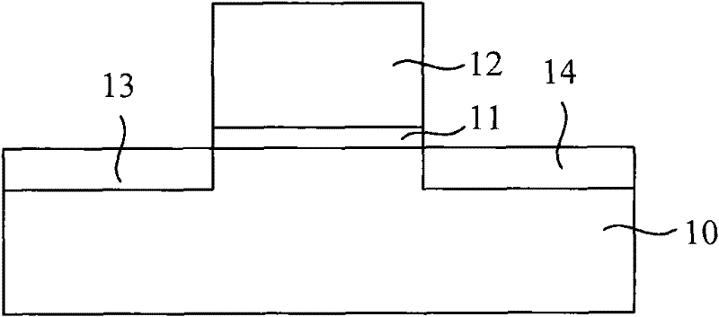
[0023] refer to Figure 5 As shown, an embodiment of the manufacturing method of the metal oxide semiconductor field effect transistor of the present invention includes:
[0024] Step s1, forming a first trench in the substrate;
[0025] Step s2, forming sidewalls on the sidewalls of the first trench;
[0026] Step s3, epitaxially growing a conductive layer in the first trench surrounded by sidewalls;
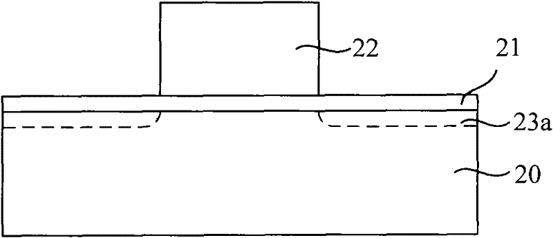
[0027] Step s4, performing light doping implantation and source / drain implantation on the substrate successively to form source / drain regions;
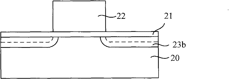
[0028] Step s5, removing the sidewall to form a second trench;
[0029] Step s6, forming a gate dielectric layer on the surface of the substrate and in the second trench;
[0030] Step s7, forming a gate on the gate dielectric layer.
[0031] In the above embodiments, before forming the gate, the source / drain regions are formed first. By adjusting the process order relative to the prior art, it is possible to avoid the influence ...
PUM
 Abstract
Description
Claims
Application Information