Manufacturing method of metal oxide semiconductor field effect transistor

An oxide semiconductor and field effect transistor technology, which is applied in semiconductor/solid-state device manufacturing, electrical components, circuits, etc., and can solve problems affecting device performance and shortening design dimensions.

Active Publication Date: 2011-07-13
SEMICON MFG INT (SHANGHAI) CORP +1
View PDF1 Cites 2 Cited by
  • Summary
  • Abstract
  • Description
  • Claims
  • Application Information

AI Technical Summary

Problems solved by technology

[0006] The invention solves the problem that the channel length is shortened relative to the design size in the manufacturing process of the metal oxide semiconductor field effect transistor in the prior art, which affects the performance of the device

Method used


Image

  • Manufacturing method of metal oxide semiconductor field effect transistor
  • Manufacturing method of metal oxide semiconductor field effect transistor
  • Manufacturing method of metal oxide semiconductor field effect transistor

Examples


Embodiment approach

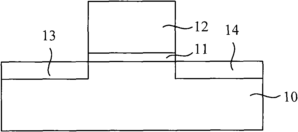
[0023] Reference Figure 5 As shown, an embodiment of the method for manufacturing a metal oxide semiconductor field effect transistor of the present invention includes:

[0024] Step s1, forming a first trench in the substrate;

[0025] Step s2, forming sidewalls on the sidewalls of the first trench;

[0026] Step s3, epitaxially grow a conductive layer in the first trench surrounded by the side wall;

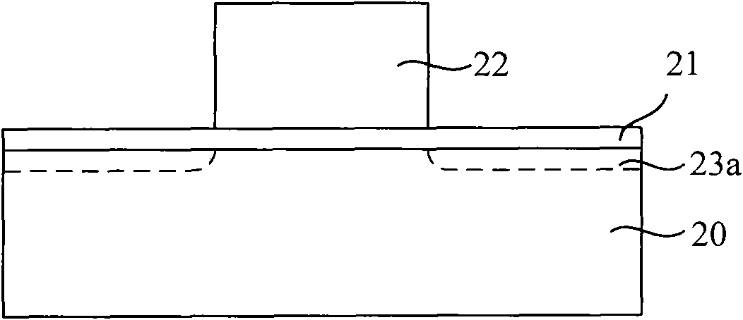
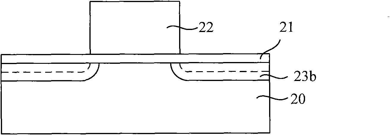
[0027] Step s4, successively perform light doping implantation and source / drain implantation on the substrate to form source / drain regions;

[0028] Step s5, removing the side wall to form a second groove;

[0029] Step s6, forming a gate dielectric layer on the surface of the substrate and the second trench;

[0030] Step s7, forming a gate on the gate dielectric layer.

[0031] In the above embodiment, before forming the gate, the source / drain regions are formed first. By adjusting the process sequence relative to the prior art, the process of the source / drain region can be prevented fr...


PUM


Abstract

The invention relates to a manufacturing method of a metal oxide semiconductor field effect transistor, which comprises the following steps of: forming a first groove in a substrate; forming a side wall on a jamb of the first groove; epitaxially growing a conductive layer in the first groove encircled by the side wall; constantly carrying out light doping injection and source / drain injection on the substrate; removing the side wall to form a second groove; forming a gate dielectric layer on the surface of the substrate and in the second groove; and forming a grid electrode on a gate oxide layer. The manufacturing method of the metal oxide semiconductor field effect transistor can effectively inhibit short channeling effect and obtain better device performance.

Description

Technical field [0001] The invention relates to the field of semiconductor device manufacturing, in particular to a method for manufacturing a metal oxide semiconductor field effect transistor. Background technique [0002] Metal Oxide Semiconductor Field Effect Transistor (MOSFET) is a semiconductor device widely used in integrated circuits. Reference figure 1 As shown, the basic structure of the metal oxide semiconductor field effect transistor includes: a substrate 10, a gate oxide layer 11 on the substrate 10, a gate electrode 12 on the gate oxide layer 11, and sources in the substrate 10 on both sides of the gate electrode 12. Area 13, drain area 14. [0003] For example, Chinese Patent Application 00134849.3 mentions a conventional manufacturing method of a metal oxide semiconductor field effect transistor, which includes forming a gate oxide layer and a gate on a substrate in sequence, and then performing light-weighting in the substrate on both sides of the gate. Doping i...

Claims


Application Information

Patent Timeline
Patent Type & Authority Applications(China)
IPC IPC(8): H01L21/336
Inventor 李奉载
Owner SEMICON MFG INT (SHANGHAI) CORP
Why Eureka
Try Eureka