Non-volatile semiconductor memory and manufacturing method thereof
a non-volatile, semiconductor technology, applied in the direction of digital storage, instruments, transistors, etc., can solve the problems of difficult to reduce the size of the memory cell, inability to ensure the effective channel length, etc., and achieve the effect of effective channel length
- Summary
- Abstract
- Description
- Claims
- Application Information
AI Technical Summary
Benefits of technology
Problems solved by technology
Method used
Image
Examples
first embodiment
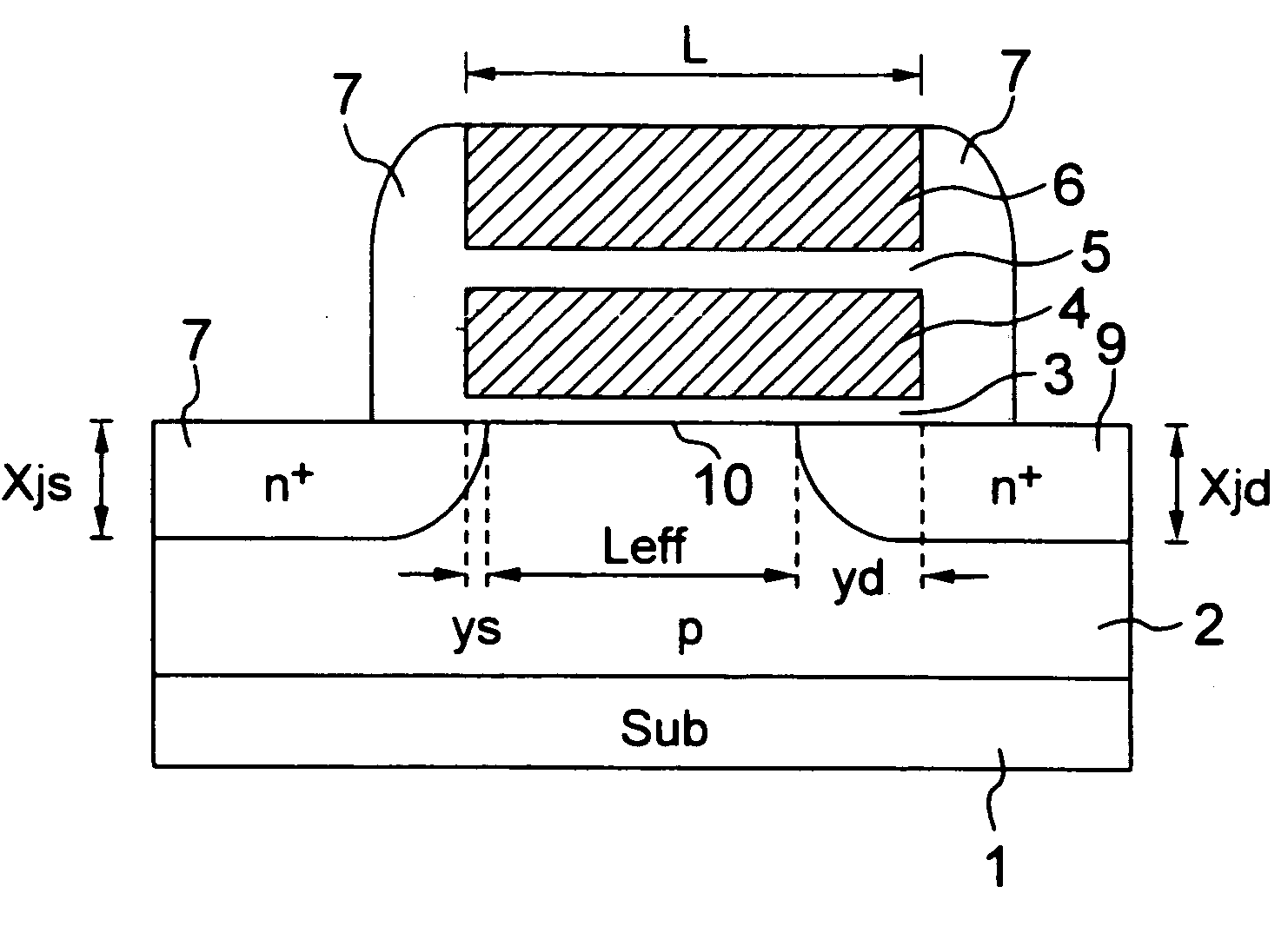
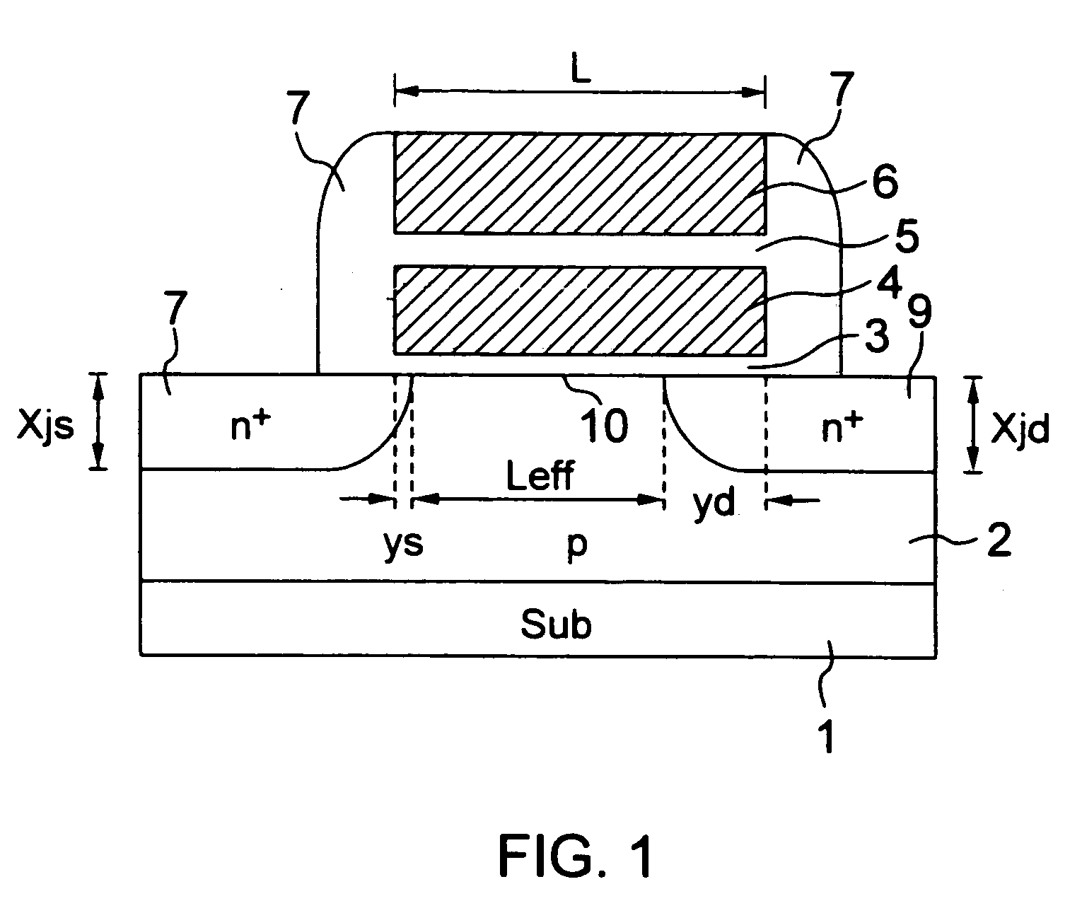
[0060]FIG. 1 shows a memory cell structure in the present invention. A p-type well 2 is provided in a memory cell region on a silicon substrate 1. The p-type well 2 is formed with a silicon oxide film 3 by thermal oxidation, serving as a tunnel insulating film. A floating gate 4 is provided on the silicon oxide film 3. A control gate 6 is further provided on the floating gate 4 through an inter-layer insulating layer 5. The control gate 6 and the floating gate 4 are patterned in the same size in a gate-lengthwise direction.
[0061] An n+ type source region 8 and a drain region 9 are formed in separate ion implantation processes. To be specific, the drain region 9 is formed by the ion implantation in self-alignment manner with a right edge of the control gate 6. A side wall insulting layer 7 is provided on side surfaces of the floating gate 4 and of the control gate 6, and the source region 8 is formed by the ion implantation in self-alignment manner with a left side surface of the sid...
second embodiment
[0078]FIG. 3 shows a structure of the non-volatile semiconductor memory cell, which is the present invention. The components corresponding to those in FIG. 1 are marked with the same numerals as those in FIG. 1. A gate structure in this embodiment is different from that in the preceding embodiment, wherein neither the floating gate 4 nor the inter-layer insulating layer 5 is formed, and an insulating layer 20 under the control gate 6 takes a 3-layered structure consisting of a silicon oxide layer (a tunnel oxide layer) 21, a silicon nitride layer 22 and a silicon oxide layer 23. This functions as an electric charge accumulating portion in which the electrons are trapped by an interface level between the silicon oxide layer 21 and the silicon nitride layer 22 of the stack-structured insulating layer 20.
[0079] In this embodiment also, the following items (1)-(3) are the same as those in the preceding embodiment.
[0080] (1) The source region 8 is provided by the ion implantation in sel...
third embodiment
[0089] Furthermore, according to the present invention, there is also a method by which the drain region is provided by the ion implantation in self-alignment with the side wall insulating layer thicker than the source region. More specifically, if the overlap of the drain region with the floating gate becomes larger than needed due to the thermal process after the ion implantation, the overlap of the drain region with the floating gate is downsized to the minimum required by implanting the ions into the drain region outwardly of the side wall insulating layer. On the other hand, if the ions are implanted on the side of the source region by use of the same side wall insulating layer, the overlap of the source region with the floating gate becomes larger than needed. Such being the case, another side wall insulating layer is further provided on the side of the source region, and the region is formed by implanting the ions outwardly of this side all.
[0090]FIGS. 6A-6D show the manufact...
PUM
 Abstract
Description
Claims
Application Information


