Method and apparatus for mapping platform-based design to multiple foundry processes

a technology of foundry process and platform, applied in the field of integrated circuits, can solve the problems of intractable computational problems, mosis does not produce the degree of performance optimality or packing density optimality required in a commercial design, and the goal tended to be very difficult in standard cell architectur

Inactive Publication Date: 2006-07-11
BELL SEMICON LLC
View PDF10 Cites 21 Cited by
  • Summary
  • Abstract
  • Description
  • Claims
  • Application Information

AI Technical Summary

Benefits of technology

[0008]According to an additional exemplary aspect of the present invention, a method for mapping platform-based design to multiple foundry processes may include the following steps. First, a first slice is optimized to a first foundry process including a first late metal step. Then, a second slice is optimized to a second foundry process including a second late metal step. The first late metal step and the second late metal step may share a functional, geometrical and electrical interface. This way, the first slice, after being implemented in the first foundry process, may be readily implemented in the second foundry process for the late metal step (or metallization), and the second slice, after being implemented in the second foundry process, may be readily implemented in the first foundry process for the late metal step (or metallization).

Problems solved by technology

However, this goal tended to be very difficult in standard cell architecture because the emphasis has been on extracting the maximum possible performance out of any particular process.
Because the problem of readily mapping an IC definition onto different fabrication processes was insufficiently constrained (too many variables) in standard cell architecture, the problem proved to be intractable computationally.
However, the extent of the detuning is such that MOSIS does not produce the degree of performance optimality or packing density optimality required in a commercial design.

Method used


Image

  • Method and apparatus for mapping platform-based design to multiple foundry processes
  • Method and apparatus for mapping platform-based design to multiple foundry processes
  • Method and apparatus for mapping platform-based design to multiple foundry processes

Examples


Embodiment Construction

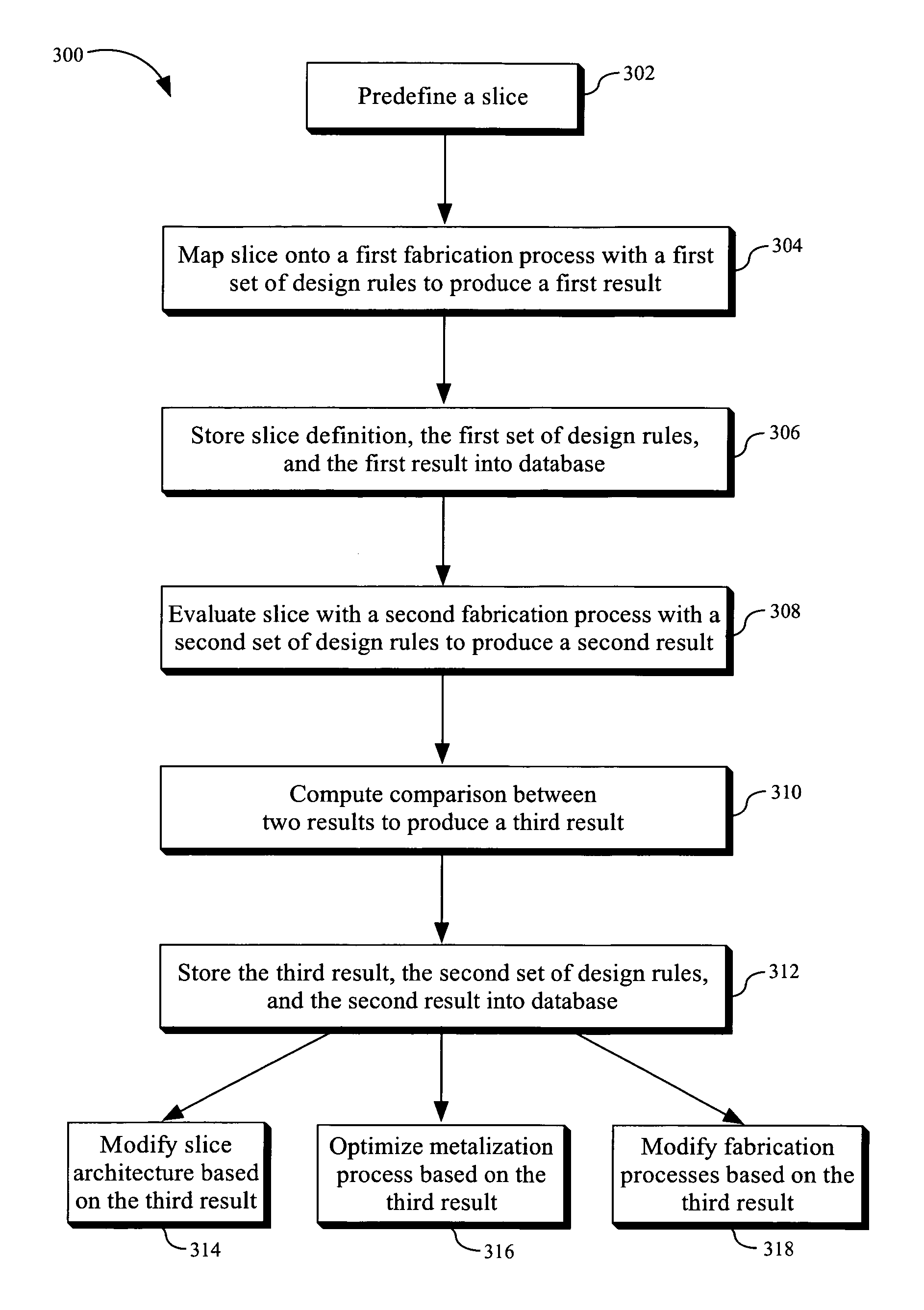
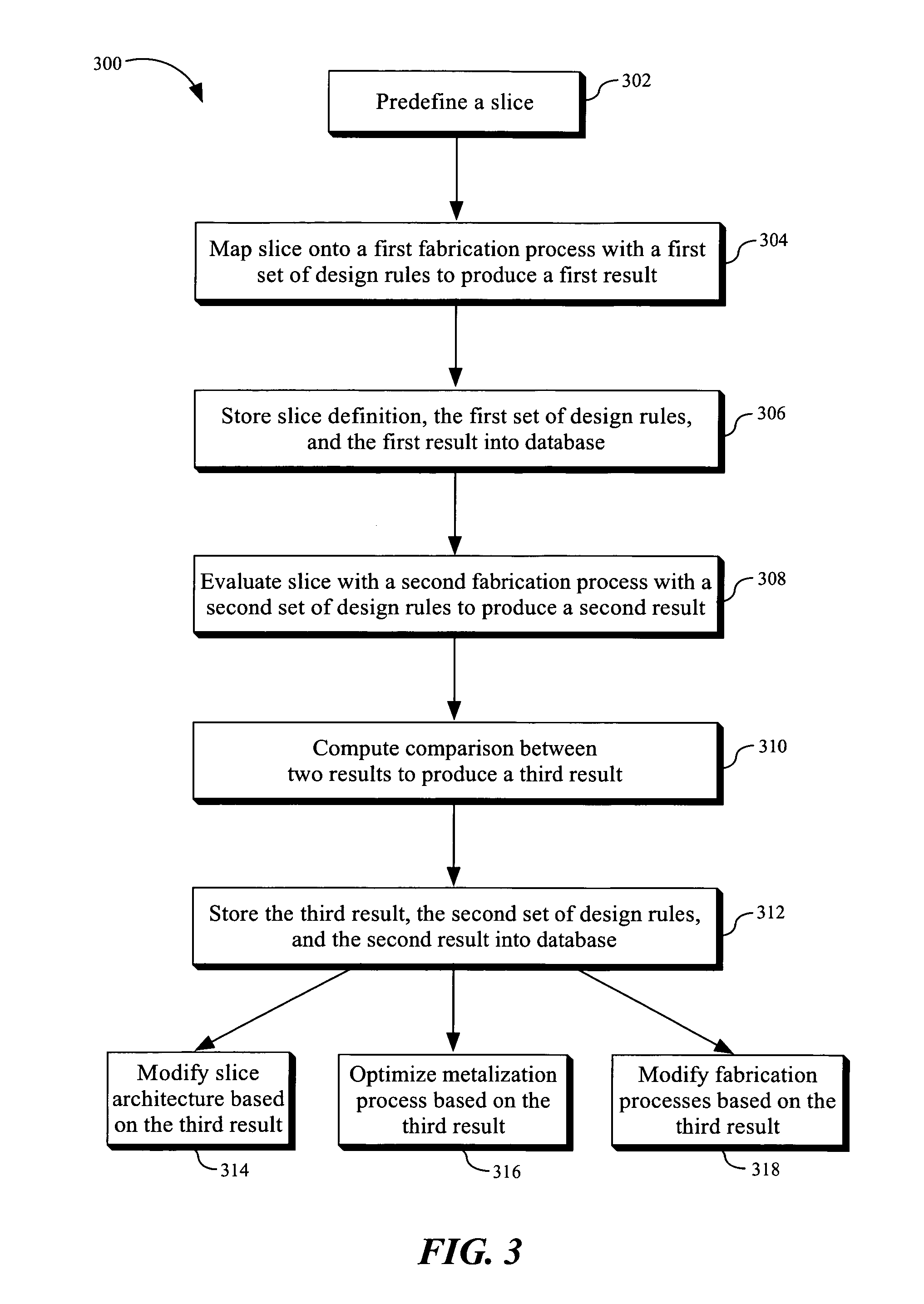
[0018]Reference will now be made in detail to the presently preferred embodiments of the invention, examples of which are illustrated in the accompanying drawings.

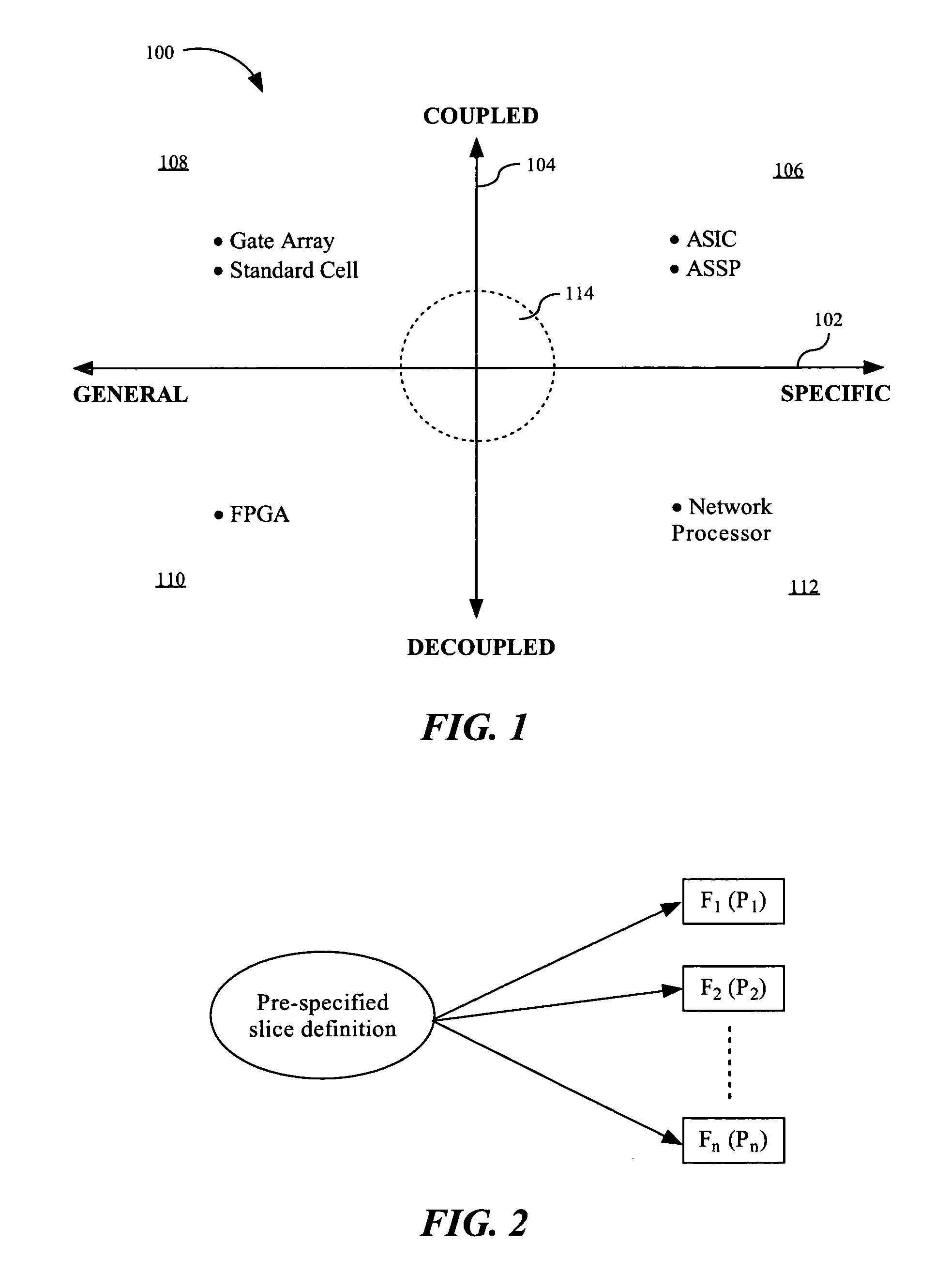
[0019]FIG. 1 is a schematic diagram illustrating a two-dimensional space 100 in which a semiconductor device may be positioned. The space 100 may include a horizontal axis 102, a vertical axis 104, and four quadrants 106, 108, 110 and 112. Using the horizontal axis 102, a distinction may be made between a semiconductor device which is general in its application and another semiconductor device which is specific in its application. Using the vertical axis 104, a distinction may be made between a semiconductor device whose final functionality is coupled to a manufacturing process and another semiconductor device whose final functionality is decoupled to (i.e., independent of) a manufacturing process, using some form of programmability.

[0020]An FPGA (field programmable gate array) is an example of a decoupled device that is v...


PUM


Abstract

The present invention is directed to a method and apparatus for mapping platform-based design to multiple foundry processes. According to an exemplary aspect of the present invention, a method for mapping platform-based design to multiple foundry processes may include the following steps. First, a virtual process is defined to include at least one fabrication process. A virtual process is a totality of variables associated with the population of candidate processes and any other process of interest, which might be purely hypothetical, that would be capable, in principle, of accommodating some or all slices. A virtual process may or may not be realized and is an abstract logical container for a population of processes. Then, the virtual process may be stored into a database. The virtual process may be in a representation including a list of attributes of entities making up the fabrication process. Next, optimization of the database may be performed using mathematical and statistical tools.

Description

CROSS REFERENCE TO RELATED APPLICATIONS[0001]The present application is a continuation-in-part of U.S. patent application Ser. No. 10 / 634,634, entitled “Method and Apparatus for Mapping Platform-Based Design to Multiple Foundry Processes,” filed Aug. 4, 2003, now pending. Said U.S. patent application Ser. No. 10 / 634,634 is herein incorporated by reference in its entirety.FIELD OF THE INVENTION[0002]This invention relates generally to integrated circuits, and particularly to a method and apparatus for mapping platform-based design to multiple foundry processes.BACKGROUND OF THE INVENTION[0003]Foundry mapping is a process of mapping an IC (integrated circuit) design onto a fabrication process used in a foundry. Different foundries conventionally have different fabrication processes and design rules. Being able to readily map an IC definition onto different fabrication processes is a long sought-after goal in the IC industry. However, this goal tended to be very difficult in standard c...

Claims


Application Information

Patent Timeline
Patent Type & Authority Patents(United States)
IPC IPC(8): G06F17/50G06F9/45
CPCG06F17/50G06F30/00
Inventor HAMLIN, CHRISTOPHER L.KOFORD, JAMES S.
Owner BELL SEMICON LLC
Why Eureka
Try Eureka