Optical scan device, image position calibration method, and image display device

a scanning device and image position technology, applied in the direction of static indicating devices, picture reproducers using projection devices, instruments, etc., can solve the problems of large scanning device size, high cost, and increased electric power of scanning devices, so as to reduce the error of projected images, improve light projection efficiency, and reduce the effect of electric power

Inactive Publication Date: 2006-07-18
SONY CORP
View PDF7 Cites 10 Cited by
  • Summary
  • Abstract
  • Description
  • Claims
  • Application Information

AI Technical Summary

Benefits of technology

[0022]A first object of the present invention is to provide a light scanning device in an image display device scanning by a one-dimensional image obtained by a one-dimensional light modulation element to generate a two-dimensional image which can improve the light projection efficiency and lower the electric power and which can reduce error of the projected image accompanying increased efficiency of light projection and a correction method of the position of an image in the light scanning device.

Problems solved by technology

For this reason, there was the problem that there was a demand for increasing the amount of the electric power of the scanning device and for raising the mechanical strength of the scan mirror.
The scanning device became large in size and expensive to realize this.

Method used


Image

  • Optical scan device, image position calibration method, and image display device
  • Optical scan device, image position calibration method, and image display device
  • Optical scan device, image position calibration method, and image display device

Examples


Embodiment Construction

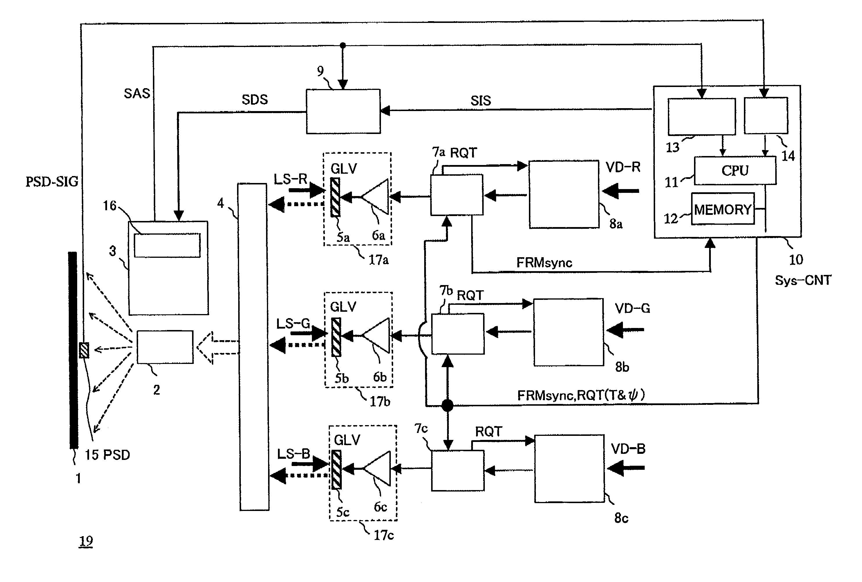
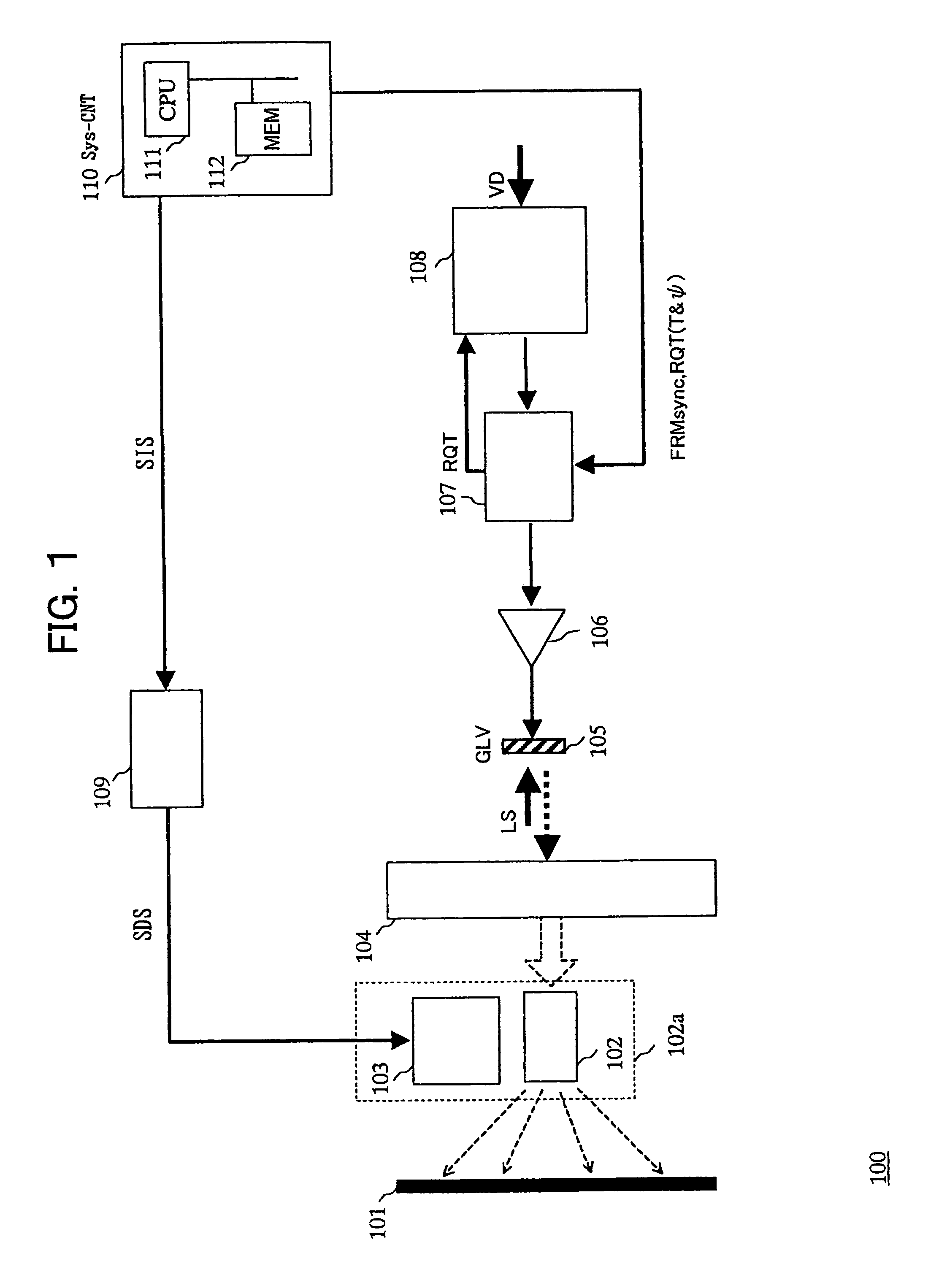
[0053]Below, an embodiment of a light scanning device of the present invention, a correction method of the position of an image, an image display method using the same, and an image display device will be explained by referring to the attached drawings.

[0054][Triangular Wave Drive System]

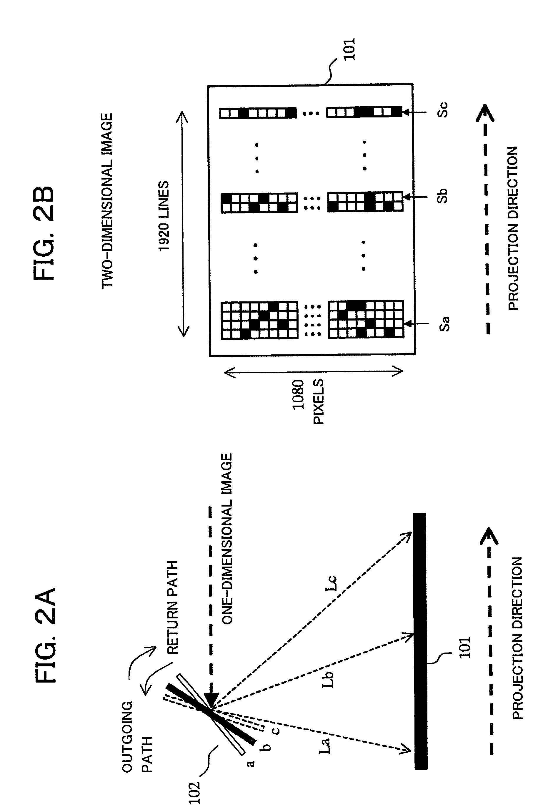
[0055]The scanning method of the present invention will be explained by referring to FIG. 4 and FIG. 5.

[0056]FIG. 4 is a view of a triangular wave signal for controlling a scanning device in the present embodiment, while FIG. 5 is a view for schematically explaining a scanning operation of a scan mirror according to the present embodiment.

[0057]Note that in the description and drawings, a “triangular wave signal” means a signal of a waveform where the rising characteristic (time and amplitude) and the falling characteristic (time and amplitude) are symmetric as illustrated in FIG. 4. Contrary to this, a “saw-tooth wave signal” means a signal of a waveform where the rising characteristic (time and am...


PUM


Abstract

An optical scanning device, a correction method of the position of an image, an image display method, and an image display device able to improve a light projection efficiency and lower the electric power and able to reduce error of the projection image along with an increase in efficiency of light projection in an image display device for scanning by a one-dimensional image to generate a two-dimensional image are provided. In the image display device, a scanning means (2) scans in both an outgoing path and a return path direction to project the light. The image display device is provided with an angle sensor 16 for reading the angle of the scanning means (2) and a position sensitive detector (15) for detecting the position of the projection light. A system control circuit (10) processes the obtained angle data and position data at an angle data correction unit (13) and a light position detection unit (14) to determine the phase delay of the output of the angle sensor (16) and adjusts a modulation / projection timing so as to correct the phase delay and match the positions of the image projected in the outgoing path and the return path.

Description

TECHNICAL FIELD[0001]The present invention relates to an optical scanning device for displaying an image based on for example a Grating Light Valve™ or other light modulation element by a projection optical system on a screen or other image displaying means, a correction method of the position of a displayed image, and an image display device using the optical scanning device.BACKGROUND ART[0002]In a projector, printer, or another image forming device, to improve the resolution of the image, there is known the method of scanning by light rays from a one-dimensional image display element by a scan mirror or other optical scanning device while projecting images onto an image forming means to form a twodimensional image (for example, refer to U.S. Pat. No. 5,982,553).[0003]As a one-dimensional pixel display device, a Grating Light Valve™ (GLV) developed by Silicon Light Machines of the U.S. is known (for example, Japanese Examined Patent Publication (Kokoku) No. 3164824 and U.S. Pat. N...

Claims


Application Information

Patent Timeline
Patent Type & Authority Patents(United States)
IPC IPC(8): G02B26/08G09G1/04G02B26/00G02B26/10G09G1/00H04N9/31
CPCH04N9/3129G02B26/105G02B5/09G02B7/1821G02B26/127
Inventor SAKAI, YOSHITSUGU
Owner SONY CORP
Why Eureka
Try Eureka