Method and apparatus for implementing power-saving sleep mode in design with multiple clock domains

Inactive Publication Date: 2006-07-18
IBM CORP
View PDF7 Cites 19 Cited by
  • Summary
  • Abstract
  • Description
  • Claims
  • Application Information

AI Technical Summary

Benefits of technology

[0015]The present invention provides a system and a method for implementing a power-saving sleep mode in a synchronous circuit core. The synchronous circuit core includes a sleep controller, a primary clock domain coupled to the sleep controller, one or more secondary clock domains, and one or more synchronization logics coupled between the primary and secondary clock domains. The primary clock domain has a primary-side idle timer and states of awake, asleep, doze, and waking. The doze and waking states are transient states between the awake and asleep states. The

Problems solved by technology

Also, because there are many different functions on a single chip, much of the time one or more of the individual core functions will be idle.
When a core is “idle” and is therefore not processing any transactions, many of that core's latches are still consuming power because they are still being clocked.
Some of these latches may feed downstream combinational logic causing those combinational gates to switch and also consume power needlessly.
Because there is often a performance penalty for “waking up” from sleep mode, cores typically have programmable counters that make them wait to assert SLEEP_REQ only if they have been idle for some reasonable programmable time.
Implementing sleep mode becomes more complex when a core has multiple clock domains.
There are several different architectures where implementing sleep mode becomes problematic.
The first problem faced is that the SLEEP_ACK signal is a primary clock domain signal and must be synchronized to the secondary domains b

Method used


Image

  • Method and apparatus for implementing power-saving sleep mode in design with multiple clock domains
  • Method and apparatus for implementing power-saving sleep mode in design with multiple clock domains
  • Method and apparatus for implementing power-saving sleep mode in design with multiple clock domains

Examples


Embodiment Construction

[0021]In the following discussion, numerous specific details are set forth to provide a thorough understanding of the present invention. However, it will be apparent to those skilled in the art that the present invention may be practiced without such specific details. In other instances, well-known elements have been illustrated in schematic or block diagram form in order not to obscure the present invention in unnecessary detail.

[0022]It is further noted that, unless indicated otherwise, all functions described herein may be performed in either hardware or software, or some combination thereof. In a preferred embodiment, however, the functions are performed by integrated circuits that are coded to perform such functions, unless indicated otherwise.

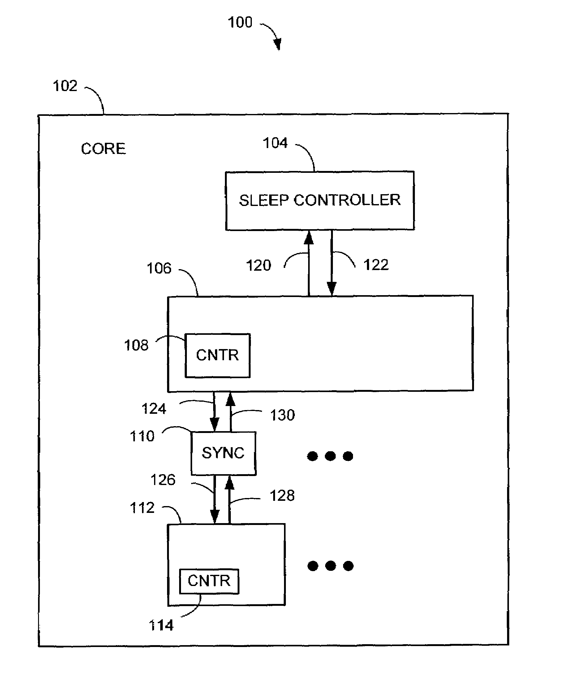
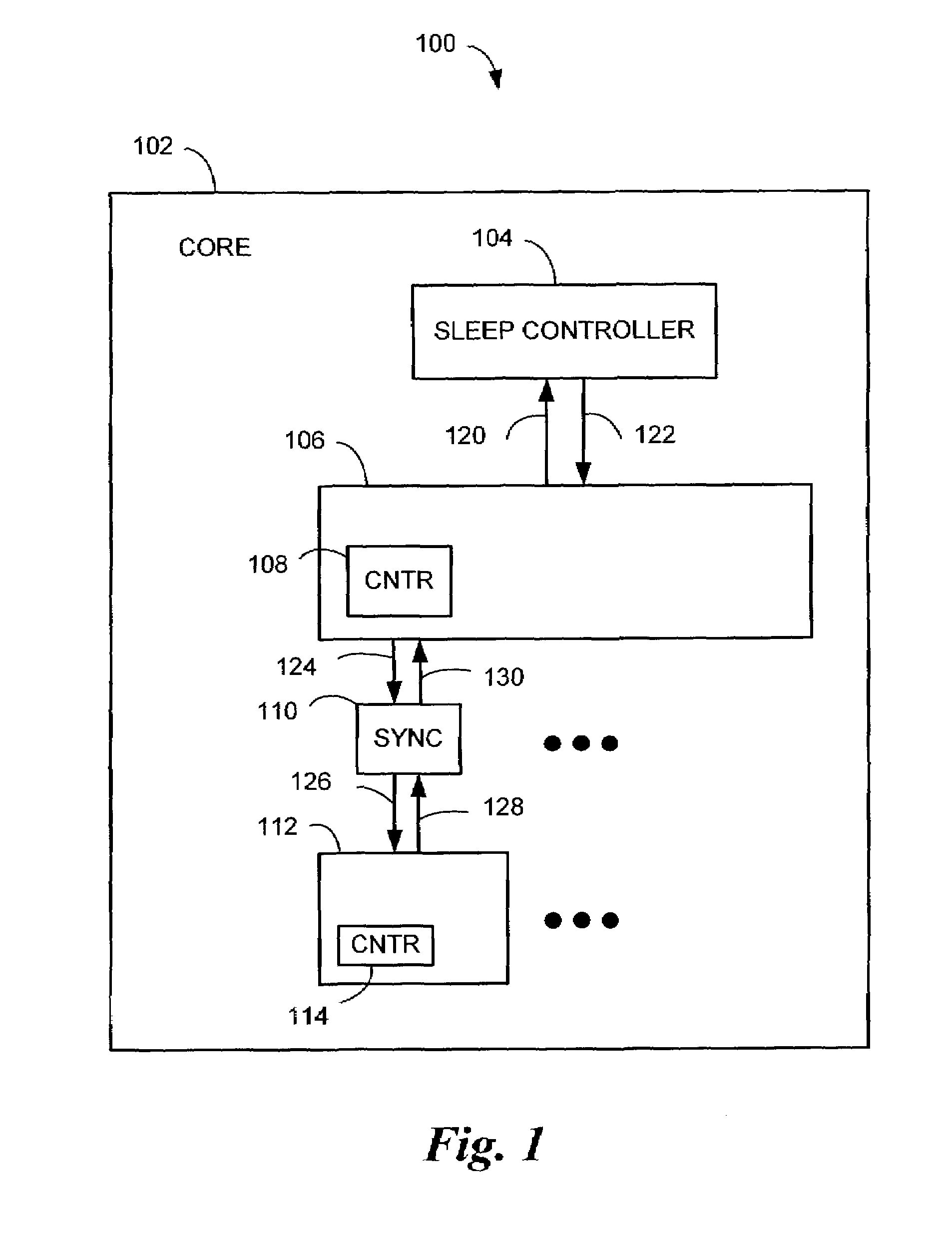
[0023]Referring to FIG. 1 of the drawings, the reference numeral 100 generally designates a synchronous digital system. A core 102 generally represents any one core of many cores in the synchronous digital system. The core 102 comprises a...


PUM


Abstract

A system and a method are provided for implementing a power-saving sleep mode in a synchronous circuit core having multiple clock domains including primary and secondary clock domains. The primary clock domain has states of awake, asleep, doze, and waking. The doze and waking states are transient states between the awake and asleep states. One or more secondary clock domains each have states of secondary awake and secondary asleep. The doze and waking states are used to eliminate race conditions between the primary and secondary clock domains. If the core has two or more secondary clock domains, the secondary clock domains each have an additional state of sleep-pending. The sleep-pending state is a transient state between the secondary awake and secondary asleep states. One or more synchronization logics are coupled between the primary and secondary clock domains.

Description

BACKGROUND OF THE INVENTION[0001]1. Field of the Invention[0002]The invention relates generally to a power-saving technique in a digital circuit and, more particularly, to a power-saving technique in a synchronous digital core design having multiple clock domains.[0003]2. Description of the Related Art[0004]Many modern synchronous circuits or system designs implement a mode called a “sleep mode,” which is a power-saving mode that the designs enter when they are essentially idle. Sleep mode is becoming increasingly common in “System On a Chip” (SOC) designs. SOCs are so named because they typically have one or more processors, one or more memory interfaces, and interfaces to various Input / Output (I / O) busses all on the same chip. SOCs are usually created out of “core” designs that are “stitched” together to make the SOC. For example, an SOC may have a plurality of cores such as a processor core, a memory core, an Ethernet core, a PCI core, serial port core, etc. Due to the large amou...

Claims


Application Information

Patent Timeline
IPC IPC(8): G06F1/26G06F1/12G06F1/32
CPCG06F1/12G06F1/324G06F1/3228Y02B60/1217Y02D10/00
Inventor BAUMGARTNER, YOANNACHADHA, SUNDEEPIACHETTA, JR., RICHARD NICHOLASLE, HIEN MINHMORROW, KIRK EDWARD
Owner IBM CORP
Why Eureka
Try Eureka