Micro-casted silicon carbide nano-imprinting stamp

a micro-casted silicon carbide and nano-imprinting technology, which is applied in the direction of fluid speed measurement, conductive pattern formation, chemical vapor deposition coating, etc., can solve the problems of reducing the imprinting stamp production cost. , to achieve the effect of strong and tough

Inactive Publication Date: 2006-07-25
APPLIED MATERIALS INC
View PDF2 Cites 23 Cited by
  • Summary
  • Abstract
  • Description
  • Claims
  • Application Information

AI Technical Summary

Benefits of technology

[0012]The micro-casted silicon carbide nano-imprinting stamp of the present invention solves the aforementioned disadvantages and limitations of the prior nano-imprinting stamps. The micro-casted silicon carbi...

Problems solved by technology

However, one of the disadvantages of the prior imprint stamp 200 is that silicon is a soft material and is subject to breakage, damage, and wear from repeated pressing steps into the mask layer 203.
In FIG. 4, a section E—E of the line feature 204 is particularly subject to wear, damage, and breakage due to repeated pressing steps.
Another disadvantag...

Method used


Image

  • Micro-casted silicon carbide nano-imprinting stamp
  • Micro-casted silicon carbide nano-imprinting stamp
  • Micro-casted silicon carbide nano-imprinting stamp

Examples


Embodiment Construction

[0032]In the following detailed description and in the several figures of the drawings, like elements are identified with like reference numerals.

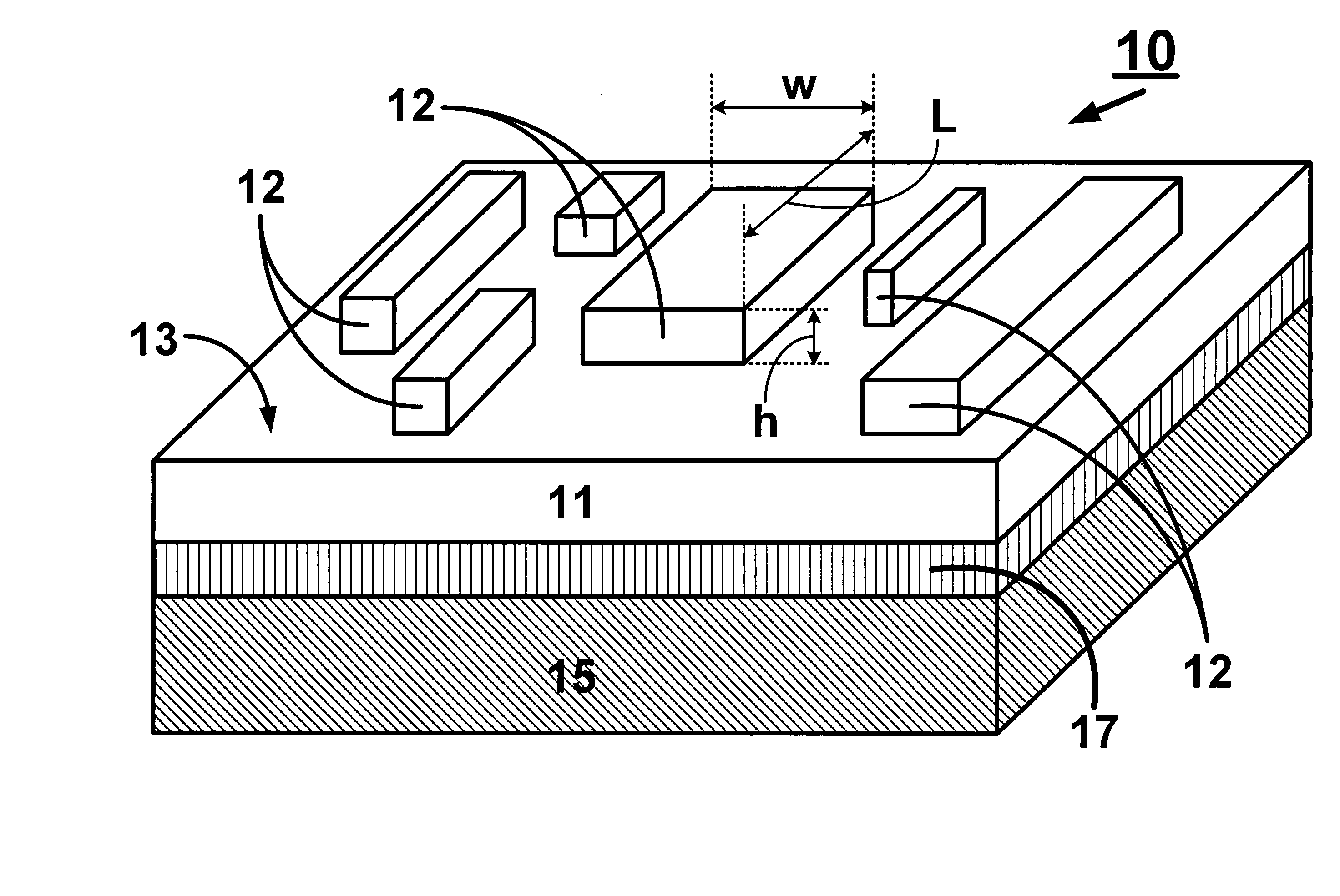
[0033]As shown in the drawings for purpose of illustration, the present invention is embodied in a micro-casted silicon carbide nano-imprinting stamp and a method of micro-casting a silicon carbide nano-imprinting stamp. The micro-casted silicon carbide nano-imprinting stamp includes a handling substrate, a glue layer connected with the handling substrate, and a foundation layer connected with the glue layer and including a base surface and a plurality of nano-sized features that are connected with the foundation layer and extend outward of the base surface. Each nano-sized feature includes an outer surface that defines an imprint profile. The foundation layer and the nano-sized features are made entirely of a material comprising silicon carbide and the foundation layer and the nano-sized features are a micro-casted unitary whole, that is,...


PUM

PropertyMeasurementUnit
Lengthaaaaaaaaaa
Nanoscale particle sizeaaaaaaaaaa

Abstract

A micro-casted silicon carbide nano-imprinting stamp and method of making a micro-casted silicon carbide nano-imprinting stamp are disclosed. A micro-casting technique is used to form a foundation layer and a plurality of nano-sized features connected with the foundation layer. The foundation layer and the nano-sized features are unitary whole that is made entirely from a material comprising silicon carbide (SiC) which is harder than silicon (Si) alone. As a result, the micro-casted silicon carbide nano-imprinting stamp has a longer service lifetime because it can endure several imprinting cycles without wearing out or breaking. The longer service lifetime makes the micro-casted silicon carbide nano-imprinting stamp economically feasible to manufacture as the manufacturing cost can be recouped over the service lifetime.

Description

[0001]This application is a division of U.S. application Ser. No. 10 / 279,643, filed Oct. 24, 2002, now U.S. Pat. No. 6,755,984.FIELD OF THE INVENTION[0002]The present invention relates generally to a structure and a method of forming a hardened nano-imprinting stamp from silicon carbide. More specifically, the present invention relates to a structure and a method of forming a hardened nano-imprinting stamp using a micro-casting process.BACKGROUND OF THE ART[0003]Nano-imprinting lithography is a promising technique for obtaining nano-size (as small as a few tens of nanometers) patterns. A key step in forming the nano-size patterns is to first form an imprinting stamp that includes a pattern that complements the nano-sized patterns that are to be imprinted by the stamp.[0004]In FIG. 1a, a prior nano-imprint lithography process includes an imprinting stamp 200 having a plurality of imprint patterns 202 formed thereon. In FIG. 1b, the imprint patterns 202 consists of a simple line and s...

Claims


Application Information

Patent Timeline
IPC IPC(8): B82B1/00B29C33/38B81B1/00B82B3/00B81C1/00C04B35/565H01L21/027H05K3/12
CPCB81C99/009B82Y10/00G03F7/0002B82Y40/00B29C2059/023Y10T428/24479H05K3/12Y10S977/887
Inventor LEE, HEONJUNG, GUN-YOUNG
Owner APPLIED MATERIALS INC
Why Eureka
Try Eureka