Method of hardening a nano-imprinting stamp

a nano-imprinting stamp and nano-imprinting technology, applied in the field of structure and method of hardening a nano-imprinting stamp, can solve the problems of reducing the cost of manufacturing the imprinting stamp b>200/b>, affecting the effect of the imprinting stamp, and being particularly subject to wear, damage, and breakag

Inactive Publication Date: 2005-07-12
HEWLETT PACKARD DEV CO LP
View PDF10 Cites 25 Cited by
  • Summary
  • Abstract
  • Description
  • Claims
  • Application Information

AI Technical Summary

Benefits of technology

[0012]The hardened nano-imprinting stamp of the present invention solves the aforementioned disadvantages and limitations of the prior nano-imprinting stamps. The silicon-based hardened nano-imprinting stamp of the present invention is made stronger and tougher by a plasma carburization and / or nitridation process that forms a hardened shell of silicon carbide (SiC), silicon nitride (SiN), or silicon carbide nitride (SiCN) along the outer surface of the hardened nano-imprinting stamp. The plasma carburization and / or nitridation process easily converts the reactive silicon (Si) material of the hardened nano-imprinting stamp into silicon carbide (SiC), silicon nitride (SiN), or silicon carbide nitride (SiCN) resulting in a hardened nano-size imprinting stamp that is much stronger than prior imprinting stamps made only of silicon.
[0013]The hardened nano-imprinting stamp has an increased lifetime and therefore the cost of manufacturing the hardened nano-imprinting stamp of the present invention can be recovered because the hardened nano-imprinting stamp can endure several more additional pressing cycles without wearing out, breaking, or being damaged, unlike the prior nano-imprinting stamps.

Problems solved by technology

However, one of the disadvantages of the prior imprint stamp 200 is that silicon is a soft material and is subject to breakage, damage, and wear from repeated pressing steps into the mask layer 203.
In FIG. 4, a section E—E of the line feature 204 is particularly subject to wear, damage, and breakage due to repeated pressing steps.
Another disadvantage of the prior imprint stamp 200 is that a cost of manufacturing the imprint stamp 200 is not recouped because the imprint stamp 200 is damaged and / or wears out before an adequate number of pressing steps required to justify the manufacturing cost of the imprint stamp 200 can occur.
Accordingly, the prior imprint stamp 200 is not economical to manufacture.

Method used


Image

  • Method of hardening a nano-imprinting stamp
  • Method of hardening a nano-imprinting stamp
  • Method of hardening a nano-imprinting stamp

Examples


Embodiment Construction

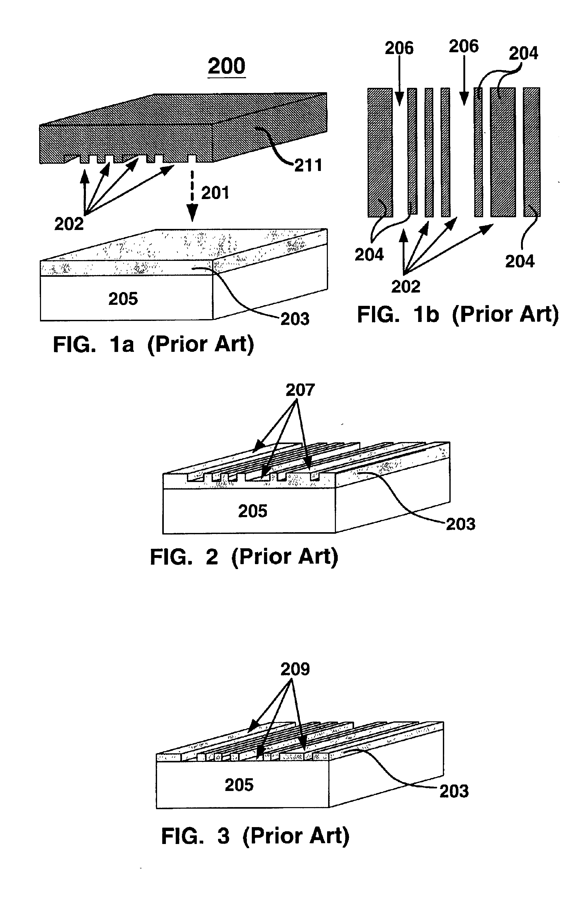
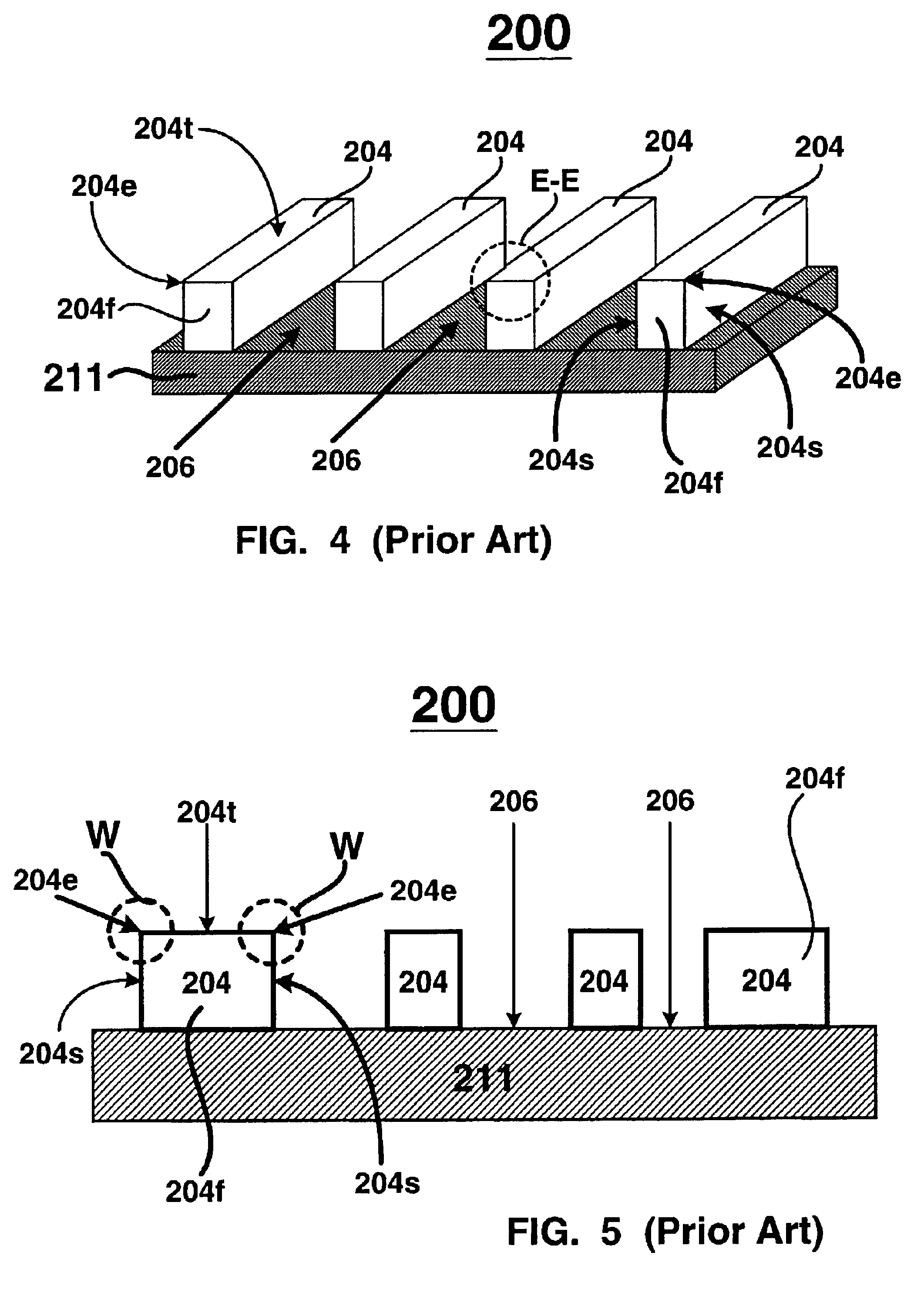
[0031]In the following detailed description and in the several figures of the drawings, like elements are identified with like reference numerals.

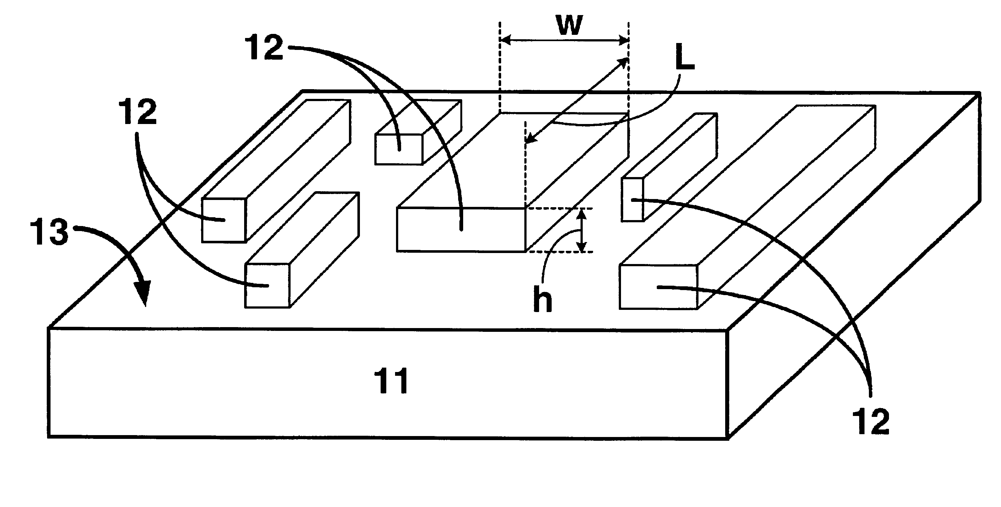
[0032]As shown in the drawings for purpose of illustration, the present invention is embodied in a hardened nano-imprinting stamp and a method of making a hardened nano-imprinting stamp. The hardened nano-imprinting stamp comprises a plurality of silicon based nano-sized features that include a hardened shell formed by a plasma carburization and / or a plasma nitridation process. A plasma with a gas comprising carbon and / or nitrogen bombards exposed surfaces of the nano-sized features and penetrates those surfaces to react with the silicon to form a silicon carbide, a silicon nitride, or a silicon carbide nitride material. The atoms of carbon and / or nitrogen only penetrate the exposed surfaces to a finite depth so that only a portion of the silicon along the exposed surfaces is converted into an outer shell of the silicon carbide, silicon ni...


PUM

PropertyMeasurementUnit
temperatureaaaaaaaaaa
depthaaaaaaaaaa
lengthaaaaaaaaaa

Abstract

A method of forming a hardened nano-imprinting stamp is disclosed. The hardened nano-imprinting stamp includes a plurality of silicon-based nano-sized features that have an hardened shell of silicon carbide, silicon nitride, or silicon carbide nitride. The hardened shell is made harder than the underlying silicon by a plasma carburization and / or a plasma nitridation process. During the plasma process atoms of carbon and / or nitrogen bombard and penetrate a plurality of exposed surfaces of the nano-sized features and chemically react with the silicon to form the hardened shell of silicon carbide, silicon nitride, or silicon carbide nitride.

Description

FIELD OF THE INVENTION[0001]The present invention relates generally to a structure and method of hardening a nano-imprinting stamp. More specifically, the present invention relates to a structure and method of hardening a nano-imprinting stamp using a plasma carburization and / or nitridation process.BACKGROUND OF THE ART[0002]Nano-imprinting lithography is a promising technique for obtaining nano-size (as small as a few tens of nanometers) patterns. A key step in forming the nano-size patterns is to first form an imprinting stamp that includes a pattern that complements the nano-sized patterns that are to be imprinted by the stamp.[0003]In FIG. 1a, a prior nano-imprint lithography process includes an imprinting stamp 200 having a plurality of imprint patterns 202 formed thereon. In FIG. 1b, the imprint patterns 202 consists of a simple line and space pattern having a plurality of lines 204 separate by a plurality of spaces 206 between adjacent lines 204. The imprint patterns 202 are ...

Claims


Application Information

Patent Timeline
Patent Type & Authority Patents(United States)
IPC IPC(8): B81C1/00B82B3/00G03F7/00H01L21/027
CPCB81C99/009B82Y10/00G03F7/0002G03F7/0017B82Y40/00Y10T428/24355
Inventor LEE, HEONJUNG, GUN-YOUNG
Owner HEWLETT PACKARD DEV CO LP
Why Eureka
Try Eureka