Charged particle beam apparatus

a technology of chargeable particles and beams, applied in the direction of individual semiconductor device testing, material analysis using wave/particle radiation, instruments, etc., can solve the problems of difficult to specify the point by using fib apparatus, insufficient measurement of contrast due to charging, and difficulty in achieving high-precision analysis. , to achieve the effect of easy-to-defect specification

Inactive Publication Date: 2006-07-25
HITACHI HIGH-TECH CORP +1
View PDF13 Cites 5 Cited by
  • Summary
  • Abstract
  • Description
  • Claims
  • Application Information

AI Technical Summary

Benefits of technology

[0009]The present invention has been accomplished to solve the above-mentioned problem, and the object of the present invention is to provide a technique, apparatus, and system that is suitable for easily specifying a defect by use of a lower analytical apparatus after the defect has been checked by use of an SEM.

Problems solved by technology

However, measurement of the contrast due to charging is insufficient for higher precision analysis.
It is desirable that the cross section of defect is observed by use of a FIB apparatus after the defect is checked on the voltage contrast image, but this technique is problematic as described herein below.
For example, when a defect point is specified by use of a SEM on a sample on which many similar bit patterns are arranged, it is difficult to specify the point by use of a FIB apparatus.

Method used


Image

  • Charged particle beam apparatus
  • Charged particle beam apparatus
  • Charged particle beam apparatus

Examples


Embodiment Construction

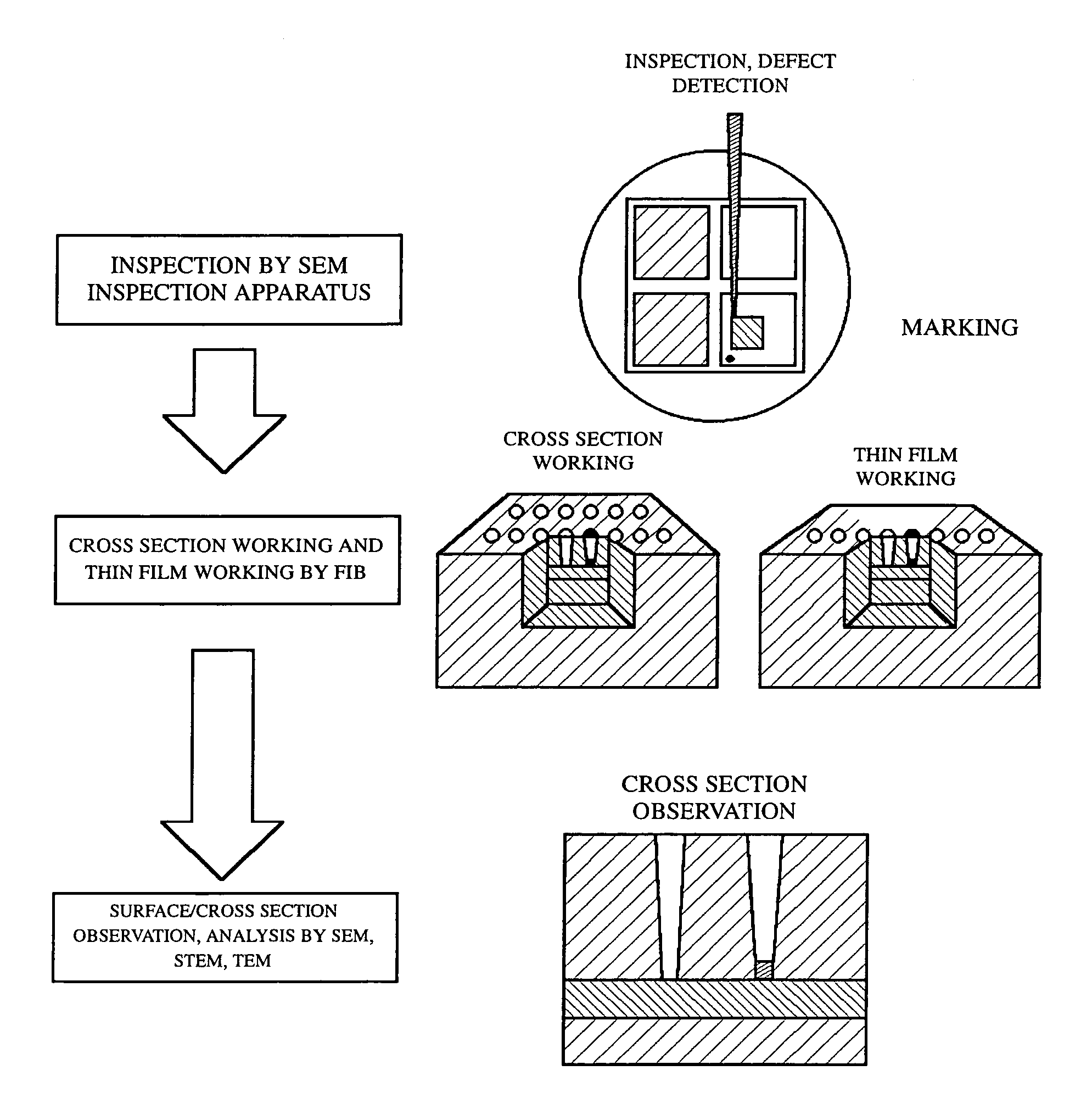
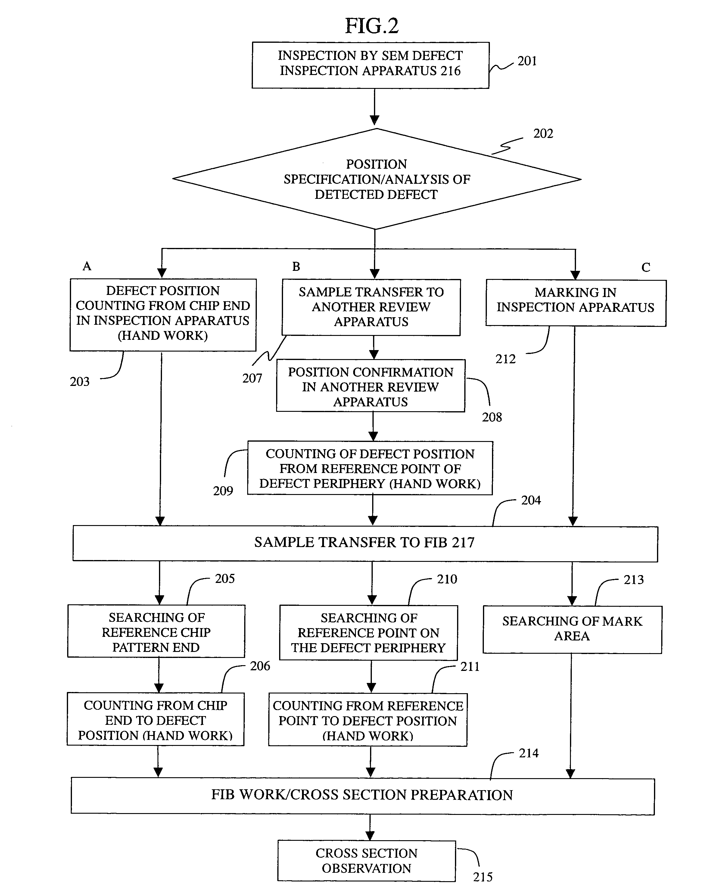
[0025]The embodiment of the present invention describes an analysis technique and a system used for applying the analysis technique to analyze the electrical defect quickly, easily, and precisely in the internal of a semiconductor device in which it is difficult to found out and analyze an electrical defect by means of the conventional apparatus, wherein the system comprises a scanning electron microscope (referred to as SEM hereinafter) that functions as an inspection apparatus for finding out the electrical defect in the internal of a semiconductor device particularly that is difficult to be found by means of other apparatus or the defect on the sample surface differently from other charged particle beam apparatus, and comprises an FIB or electron microscope for analyzing the electric defect more in detail that has been found by means of the above-mentioned inspection apparatus.

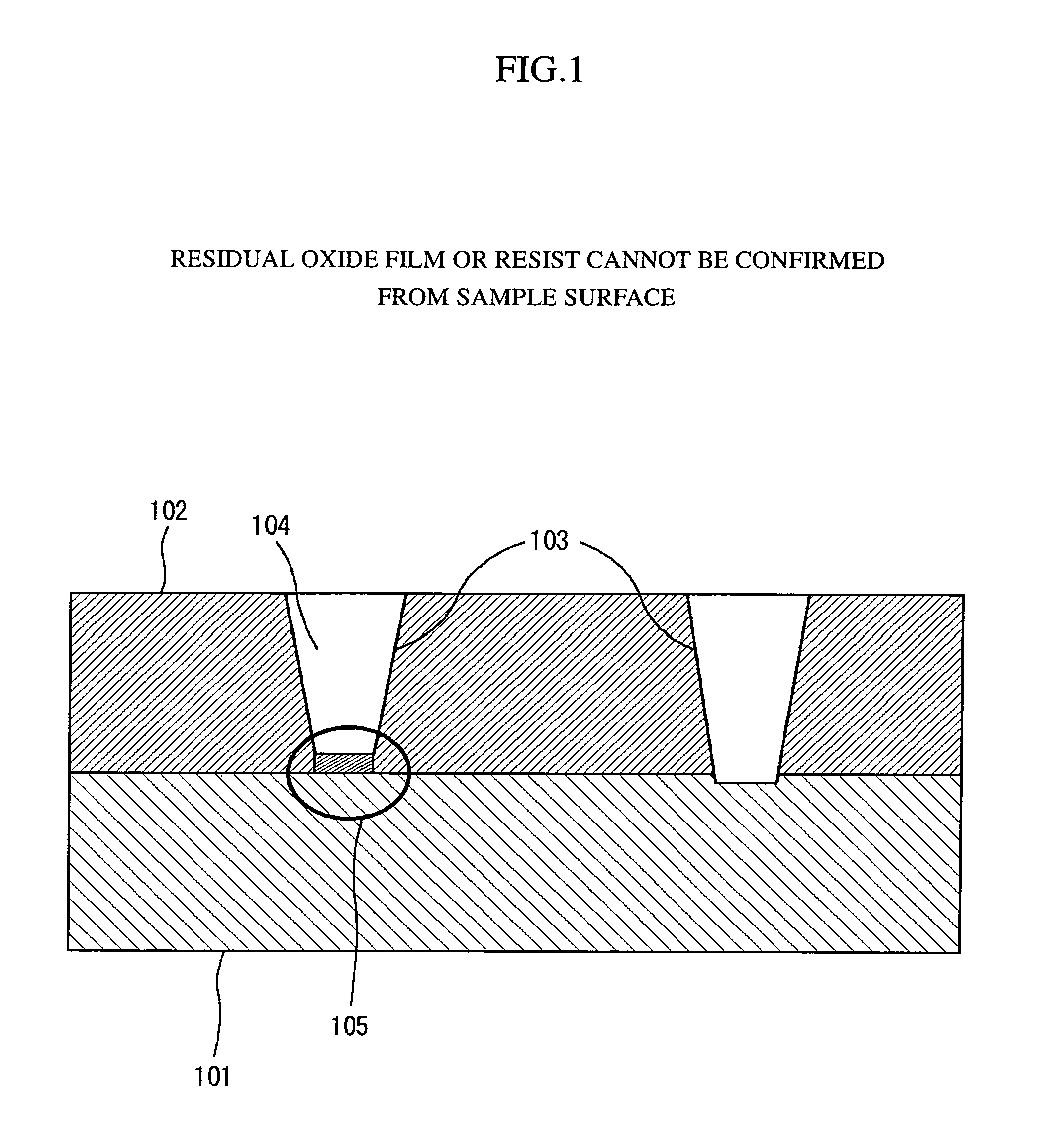
[0026]An electron beam inspection system can sensitively detect an electrical defect (voltage contrast) ...


PUM

PropertyMeasurementUnit
temperatureaaaaaaaaaa
circuit densityaaaaaaaaaa
defect inspectionaaaaaaaaaa

Abstract

The object of the present invention is to transmit the position information of a defect that has been specified by means of a circuit pattern inspection apparatus quickly and precisely so that the position information is efficiently used in another apparatus. Marking is carried out on the peripheral area of the defect by use of a charged particle beam irradiation mechanism of the inspection apparatus. The marking realizes sharing of the defect position information with another apparatus. The marking technique includes deposition of a deposit and charging up by means of irradiation of a charged particle beam. The marking in the inspection apparatus allows the defect position information to be transmitted to another apparatus more correctly and easily, and as a result, analysis accuracy is improved and analysis time is shortened.

Description

BACKGROUND OF THE INVENTION[0001]1. Field of the Invention[0002]This invention relates to a technique suitable for sample analysis of semiconductor devices in which it is difficult to analyze the defect in depth from the surface.[0003]2. Description of Related Art[0004]Higher circuit density has been required with progress of higher circuit integration of devices. Actually, defect inspection apparatus for inspecting semiconductor devices is required to analyze not only the defect information on the surface but also the defect / foreign-particle information in the internal of a sample.[0005]For such analysis, the analysis of defect / foreign-particle on the surface and analysis of cross-section image for analyzing internal defect / foreign-particle are carried out on the positional information obtained by means of an inspection apparatus by use of a focused ion beam apparatus (FIB), scanning electron microscope (SEM), and transmission electron microscope (TEM).[0006]For example, in the cas...

Claims


Application Information

Patent Timeline
Patent Type & Authority Patents(United States)
IPC IPC(8): G01N23/00G01R31/25G01R31/305G21K7/00G01N23/225H01J37/28
CPCH01J37/261G01N23/225H01J37/28H01J2237/2817
Inventor FURIKI, MASANARIKUROSAWA, KOUICHIKONNO, TAKEHIKOFUNATSU, RYUICHI
Owner HITACHI HIGH-TECH CORP
Why Eureka
Try Eureka