Dimension measurement approach for metal-material

Inactive Publication Date: 2006-08-08
THE BOARD OF TRUSTEES OF THE LELAND STANFORD JUNIOR UNIV
View PDF14 Cites 18 Cited by
  • Summary
  • Abstract
  • Description
  • Claims
  • Application Information

AI Technical Summary

Benefits of technology

[0013]The above summary is not intended to describe each illustrated embodiment or every implementation of the p

Problems solved by technology

Recent technological advances in the semiconductor industry have permitted dramatic increases in circuit density and complexity, and commensurate decreases in power consumption and package sizes for integrated circuit devices.
These and other demands have led to increased pressure to manufacture a large number of semiconductor devices at a rapid pace while increasing the complexity and improving the reliability of the devices.
Optical techniques that have previously been available for th

Method used


Image

  • Dimension measurement approach for metal-material
  • Dimension measurement approach for metal-material
  • Dimension measurement approach for metal-material

Examples


Embodiment Construction

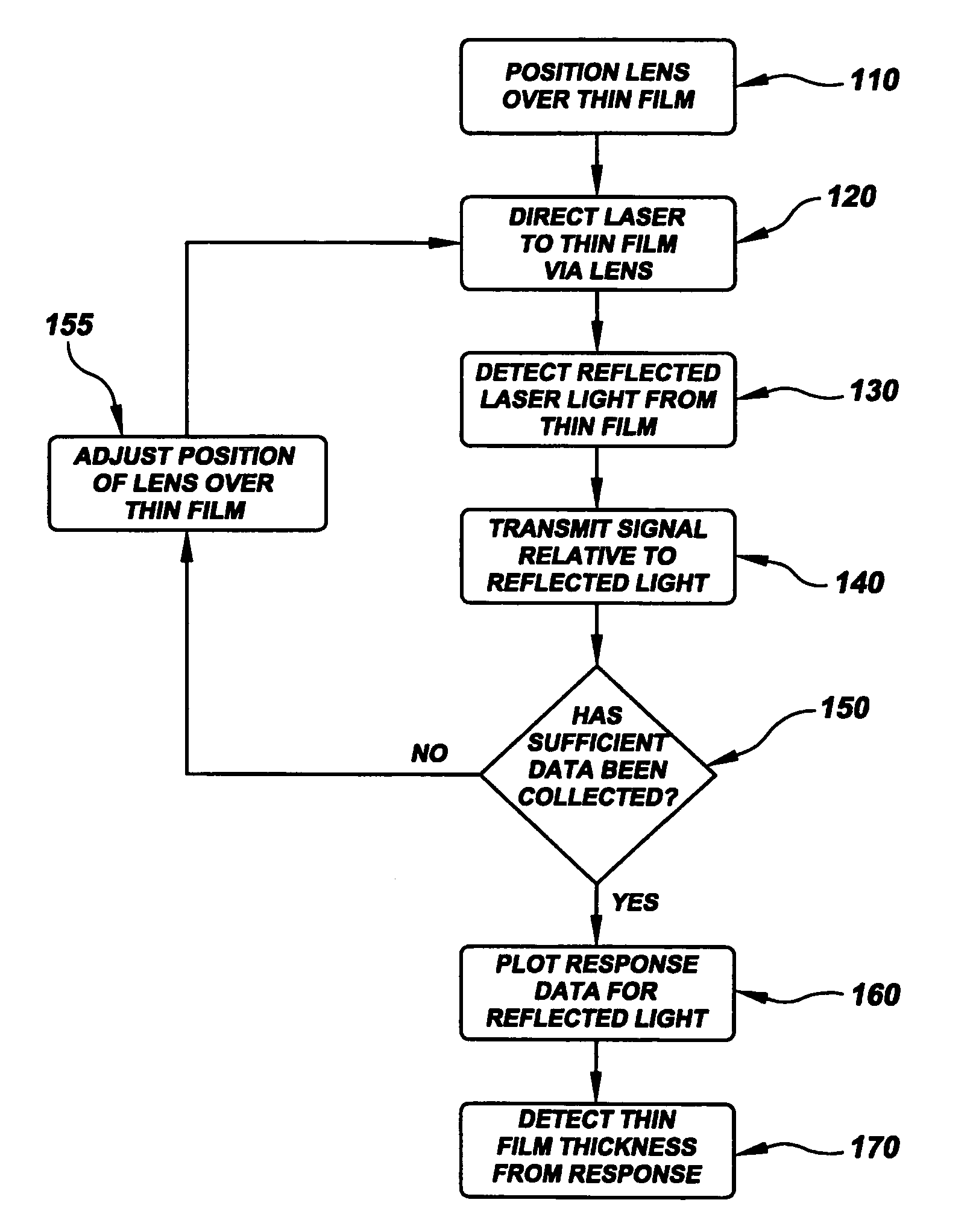
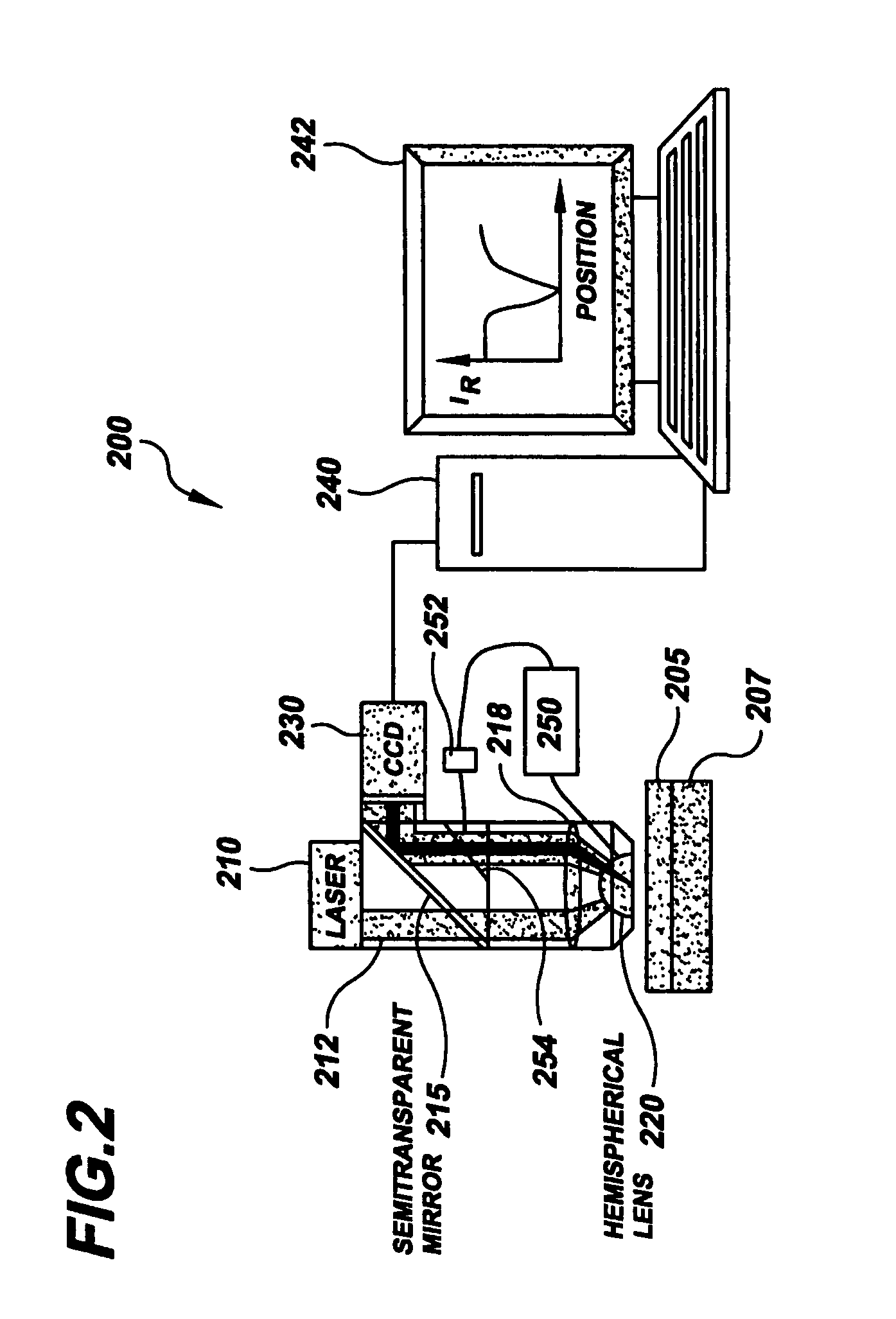
[0019]The present invention is believed to be applicable to a variety of different types of devices and processes, and the invention has been found to be particularly suited for semiconductor devices, analysis and manufacture involving approaches to the measurement of a variety of structural dimensions. While the present invention is not necessarily limited to such applications, various aspects of the invention may be appreciated through a discussion of various examples using this context.

[0020]According to an example embodiment of the present invention, an optical approach involving light excitation is used for measuring physical dimensions of a structure. Plasmon-exciting light is directed at a structure and electrons therein are excited. A characteristic of reflected light related to the electron excitation is used to identify a dimensional parameter of the structure.

[0021]According to a more particular example embodiment of the present invention, a non-invasive optical approach ...


PUM


Abstract

Dimensional parameters of metal-containing structures such as films, interconnects, wires and stripes, and nanoparticles are detected using an approach involving plasmon-excitation and one or more metal-constituency characteristics of the metal-containing structures. According to an example embodiment of the present invention, plasmon-exciting light is used to excite plasmons in a structure, the plasmon excitation being responsive to the metal constituency. A characteristic of light reflected from the structure is then used to detect dimensional parameters of the structure. In one implementation, a characteristic of the reflected light that is related to the state of plasmon excitation in the structure is used to detect the dimensional parameters. In another implementation, the angle of incidence of the plasmon-exciting light is used in connection with an intensity-related characteristic of light reflected from structure to detect one or more dimensions of the structure. In still another implementation, the intensity of different wavelengths of the reflected light is used to determine one or more dimensions of the structure. With these approaches, the dimensions of a variety of structures such as metal films, interconnects, wires, and stripes are determined.

Description

RELATED PATENT DOCUMENTS[0001]This patent document is related to Provisional Patent Application Ser. No. 60 / 425,097, filed on Nov. 8, 2002 (STFD.054P1), to which Applicant claims priority for common subject matter under 35 U.S.C. §120.FIELD OF THE INVENTION[0002]The present invention relates generally to metal-containing structures, such as metal nanoparticles, metallic nanowires and stripes, and thin metallic films and more particularly to the measurement of structural dimensions of the metal-containing structures and involving devices and approaches therefor.BACKGROUND[0003]Recent technological advances in the semiconductor industry have permitted dramatic increases in circuit density and complexity, and commensurate decreases in power consumption and package sizes for integrated circuit devices. Single-chip microprocessors now include many millions of transistors operating at speeds of hundreds of millions of instructions per second to be packaged in relatively small, air-cooled ...

Claims


Application Information

Patent Timeline
IPC IPC(8): G01N21/55
CPCG01B11/0616G01N21/553G01N21/554
Inventor BRONGERSMA, MARK L.
Owner THE BOARD OF TRUSTEES OF THE LELAND STANFORD JUNIOR UNIV
Why Eureka
Try Eureka