

Three-dimensional tomography
a three-dimensional tomography and semiconductor technology, applied in the direction of material analysis, material analysis using wave/particle radiation, instruments, etc., can solve the problems of increasing the density and complexity of the integrated circuit, requiring a highly complex and expensive manufacturing process, and reducing the power consumption and package size. , to achieve the effect of improving the ability to detect, locate and identify
- Summary
- Abstract
- Description
- Claims
- Application Information
AI Technical Summary
Benefits of technology
Problems solved by technology
Method used
Image

Examples
Embodiment Construction
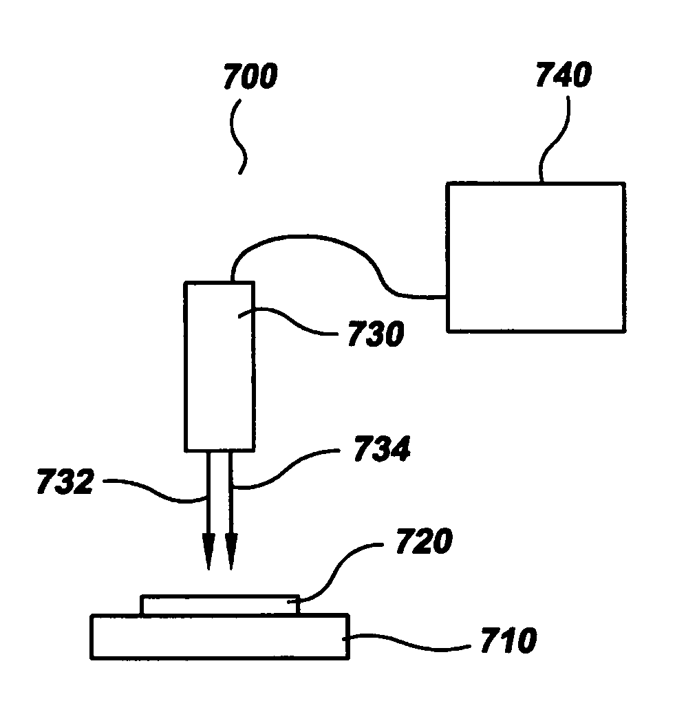
[0019]The present invention is believed to be applicable to a variety of different types of semiconductor devices, and has been found to be particularly suited for defect analysis in semiconductor dies. While the present invention is not necessarily limited to such devices, various aspects of the invention may be appreciated through a discussion of various examples using this context.
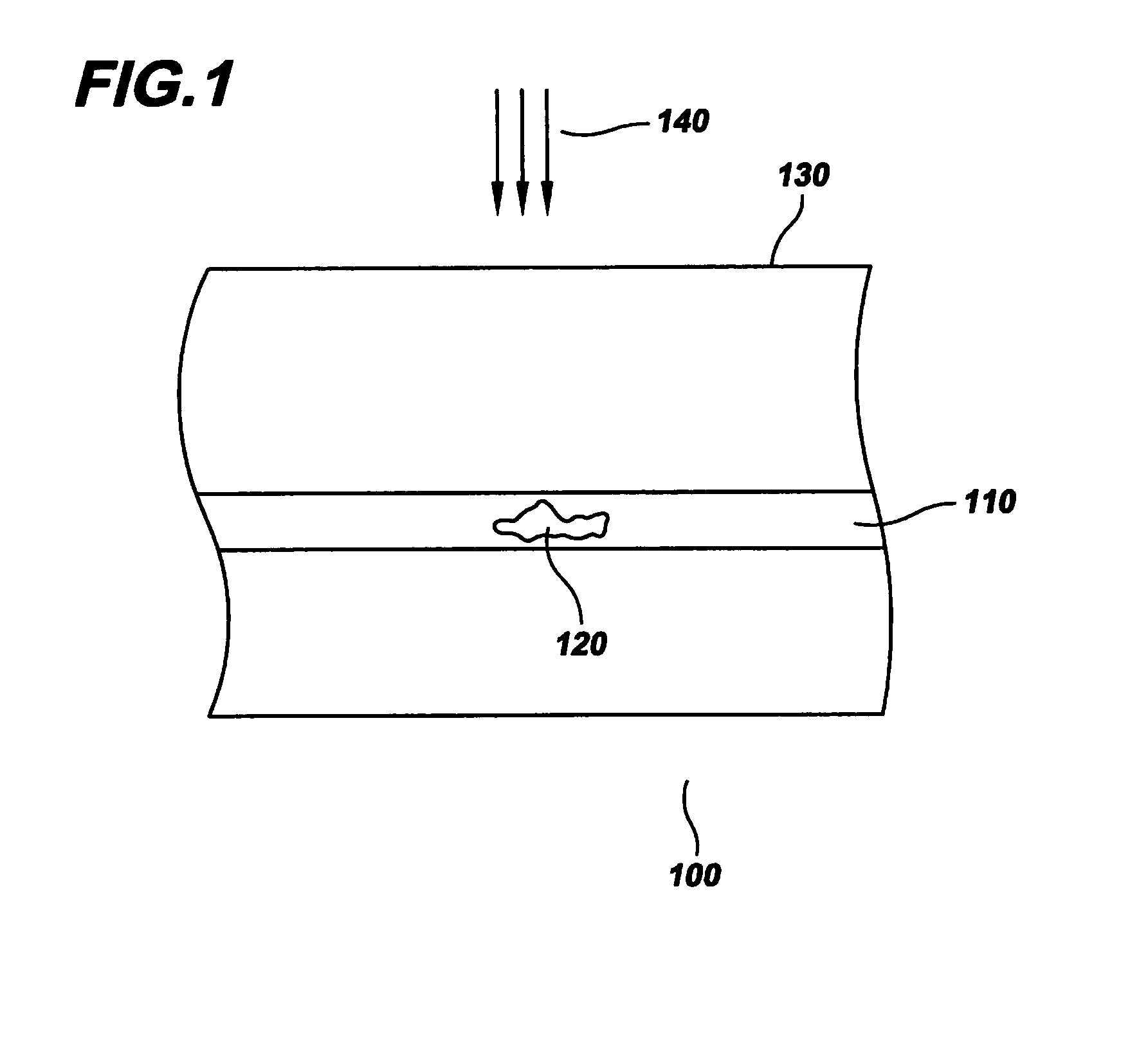
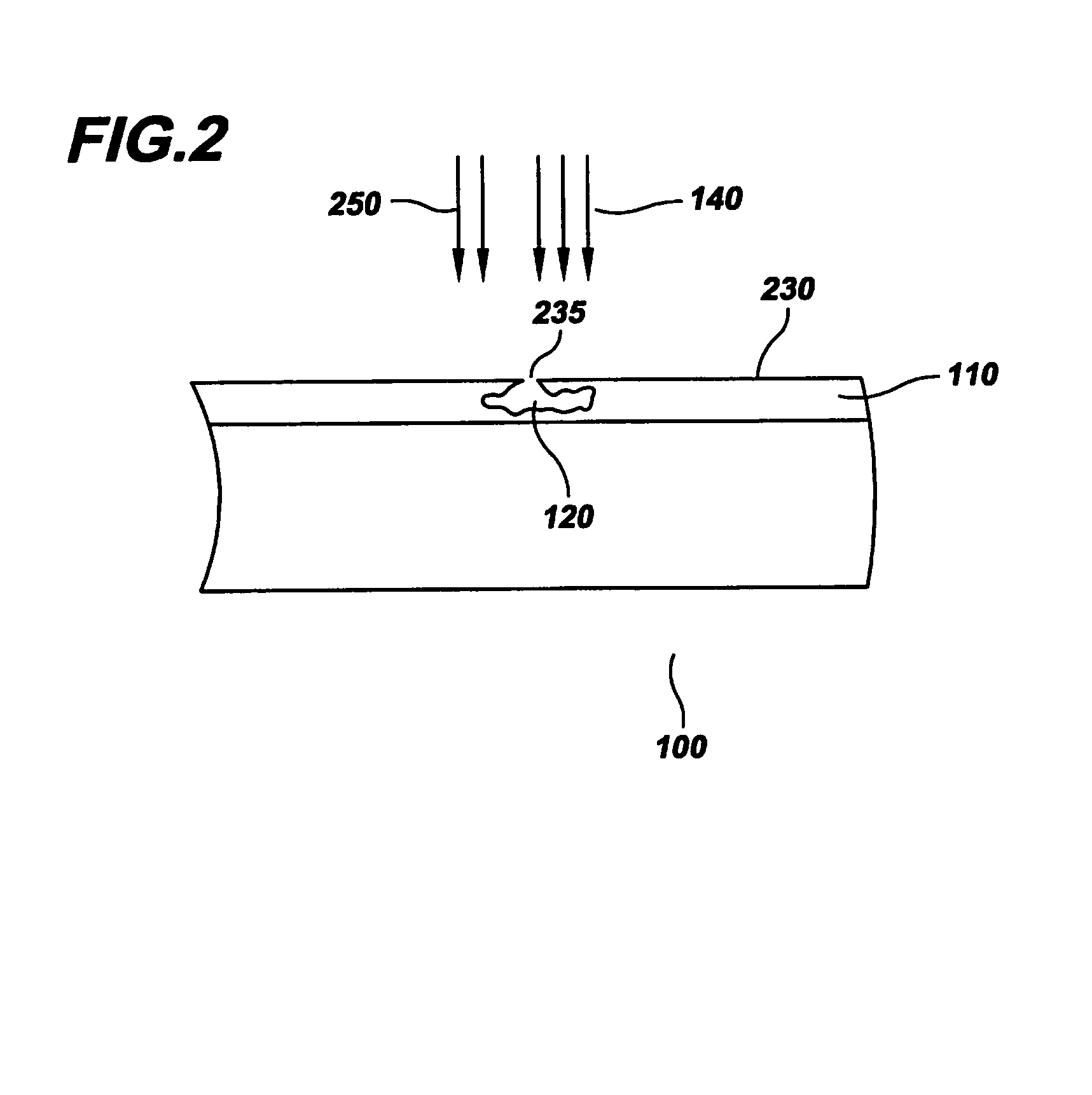
[0020]According to an example embodiment of the present invention, a semiconductor die having a defect, such as a defective electrical contact, a void, an open circuit or a short circuit is analyzed. Substrate is removed from a selected portion of the die having a suspected defect, and is removed in both horizontal and vertical directions as desired. The substrate removal uses commonly-available removal techniques, such as, for example, chemical-mechanical polishing (CMP), laser etching and focussed ion beam (FIB) etching. In addition, the extent of substrate removed is selected based on the application...
PUM
 Abstract
Description
Claims
Application Information