Multilayer chip capacitor

a multi-layer chip and capacitor technology, applied in the direction of capacitors, fixed capacitor details, fixed capacitors, etc., can solve the problems of difficult to meet the target impedance, the reduction of the esl does not meet the level required, and the inability to design the power distribution network stably

Active Publication Date: 2006-08-15
SAMSUNG ELECTRO MECHANICS CO LTD
View PDF13 Cites 37 Cited by
  • Summary
  • Abstract
  • Description
  • Claims
  • Application Information

AI Technical Summary

Benefits of technology

[0014]Therefore, the present invention has been made in view of the above problems, and it is an object of the present invention to provide a multilayer chip capacitor, which reduces the ESL component generated due to current flowing through external electrodes from the bottom surface of the capacitor.
[0015]It is another object of the present invention to provide a multilayer chip capacitor, which has a sufficient overall thickness, thereby reducing mechanical damage and having an improved production yield.
[0016]It is still another object of the present invention to provide a mutilayer chip capacitor, which can prevents the ESR from reducing extremely and control the ESR easily.
[0019]Since the thickness of the lower dummy layer is smaller than the thickness of the upper dummy layer, the multilayer chip capacitor has a reduced ESL value as well as a sufficient mechanical strength.
[0022]In accordance with one embodiment of the present invention, thin dielectric layers are formed between the plural internal electrodes; and the upper and lower dummy layers are made of the same material as that of the thin dielectric layers. In this case, since the thickness of the upper dummy layer is larger than the thickness of the lower dummy layer, the mechanical strength of the capacitor is improved.
[0023]In accordance with another embodiment of the present invention, thin dielectric layers are formed between the plural internal electrodes; and the upper dummy layer includes: an upper dummy dielectric layer made of the same material as that of the thin dielectric layers; and an upper reinforcing layer formed on the upper dummy dielectric layer and made of the different material from that of the thin dielectric layers. The upper reinforcing layer increases the overall thickness of the capacitor, and improves the mechanical strength of the capacitor. The upper reinforcing layer is made of plastic, glass, or ceramic.

Problems solved by technology

However, such reduced amount of the ESL does not satisfy the level required for the decoupling capacitors for high frequency circuit.
If the ESR is extremely small, it is hard to meet the target impedance and impossible to design power distribution network stably.
However, according to the U.S. Patent, the ESL is increased, and the ESR is not controllable.
However, when the multilayer chip capacitor is excessively thin, the mechanical strength of the multilayer chip capacitor is decreased.
For example, when the multilayer chip capacitor is designed to have a thickness of less than 0.3 mm, the capacitor is easily broken or damaged during the manufacturing process thereof, thus deteriorating a production yield of chip capacitors.
Particularly, the above mechanical damage of the capacitor is highly generated when the capacitor main body is polished after sintering or when the manufactured multilayer chip capacitor is mounted on a substrate.

Method used


Image

  • Multilayer chip capacitor
  • Multilayer chip capacitor
  • Multilayer chip capacitor

Examples


example

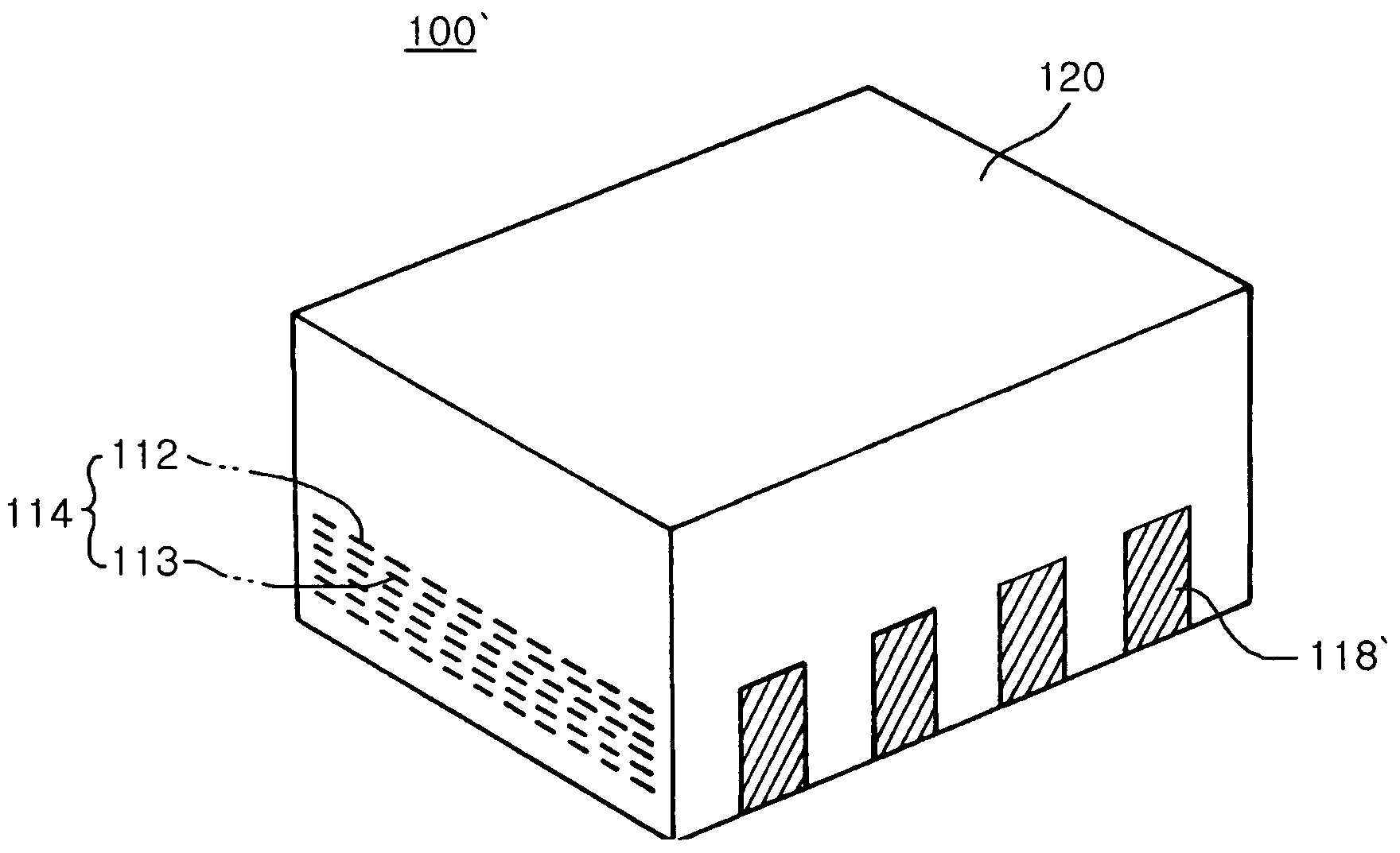
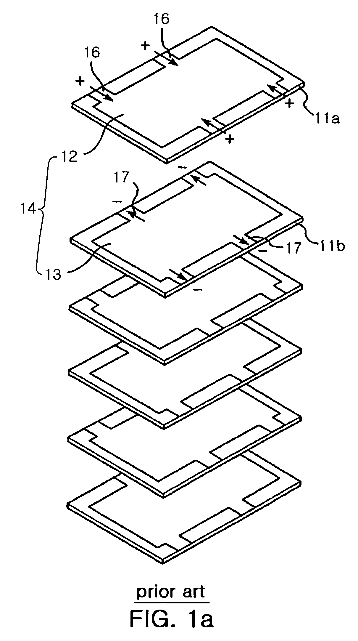
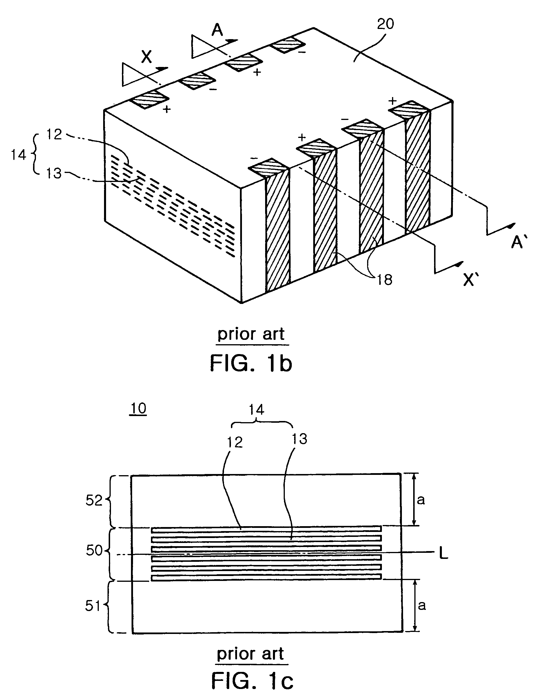
[0091]The applicant performed an experiment, which compared ESL characteristics of a conventional multilayer chip capacitor and multilayer chip capacitors in accordance with three examples (a first though third examples) of the present invention in order to inspect the improvement of the ESL characteristics of the multilayer chip capacitors of the present invention. The conventional multilayer chip capacitor has the internal electrode structure shown in FIG. 1a and the symmetrical sectional structure shown in FIG. 1c. The capacitors of the first through third examples have the internal electrode structure shown in FIG. 13. The multilayer chip capacitor of the first example has the lower-upper asymmetrical sectional structure shown in FIG. 4, the capacitor of the second example has the lower-upper asymmetric sectional structure shown in FIG. 10, and the capacitor of the third example has the lower-upper symmetric sectional structure shown in FIG. 11. All of the conventional multilaye...


PUM


Abstract

A multilayer chip capacitor, which reduces ESL generated due to current flowing through external electrodes and assures an improved mechanical strength. The multilayer chip capacitor includes an upper dummy layer and a lower dummy layer; a plurality of internal electrodes interposed between the upper and lower dummy layers; and external electrodes connected to the internal electrodes, wherein the thickness of the lower dummy layer is smaller than the thickness of the upper dummy layer.

Description

RELATED APPLICATIONS[0001]The present invention is based on, and claims priority from, Korean Application Number 2005-5513, filed Jan. 20, 2005, and Korean Application Number 2005-16874, filed Feb. 28, 2005, the disclosures of which are incorporated by reference herein in their entirety.BACKGROUND OF THE INVENTION[0002]1. Field of the Invention[0003]The present invention relates to a multilayer chip capacitor, and more particularly to a multilayer chip capacitor, which has a low equivalent serial inductance (ESL) in a high frequency circuit.[0004]2. Description of the Related Art[0005]Generally, multilayer chip capacitors have a small size, achieve high capacitance, and are easily mounted on a substrate, thus being widely used in various electronic apparatuses. Multilayer chip capacitors are used as capacitive components of high frequency circuits, particularly as decoupling capacitors arranged in power supply circuits of LSI. In order to use a multilayer chip capacitor in a high-fr...

Claims


Application Information

Patent Timeline
Patent Type & Authority Patents(United States)
IPC IPC(8): H01G4/06H01G4/005H01G4/228
CPCH01G4/30H01G4/232
Inventor LEE, BYOUNG HWASHIM, CHANG HOONCHUNG, HAE SUKPARK, DONG SEOKPARK, SANG SOOPARK, MIN CHEOL
Owner SAMSUNG ELECTRO MECHANICS CO LTD
Why Eureka
Try Eureka