Alkaline solution and manufacturing method, and alkaline solution applied to pattern forming method, resist film removing method, solution application method, substrate treatment method, solution supply method, and semiconductor device manufacturing method

a technology alkaline solution applied in the field of alkaline solution and manufacturing method, can solve the problems of large problems, insufficient wettability with respect, and the development solution is not easily diffused between the reaction product and the photosensitive resist surface, and achieves the effect of reducing properties

Inactive Publication Date: 2006-08-29
KK TOSHIBA
View PDF23 Cites 1 Cited by
  • Summary
  • Abstract
  • Description
  • Claims
  • Application Information

AI Technical Summary

Benefits of technology

[0239]The hydrogen molecules have an action of reducing the resist surface upon contacting the resist surface. Therefore, the difference of the affinity of the exposed portion surface and unexposed portion surface for the developing solution is alleviated. Thereby, the difference of the developing speed locally generated during the development is reduced, and the size uniformity after the development is enhanced.
[0247]When the hydrogen molecules are contained in the developing solution, the hydrogen molecules have an effect of modifying the reaction products, or the surface state of the resist. Thereby, the degree of the intermolecular interaction between the reaction products can be weakened, and the hydrogen molecules in the developing solution can inhibit the reaction products from cohering. That is, the amount of reaction products again adhering to the resist surface is decreased, and the amount of defects caused by re-adhesion of the cohering reaction products to the resist surface is largely suppressed.
[0250]When the oxidizing solution is used as the cleaning solution, the organic particles are oxidized / decomposed, and diffused in the solution. Therefore, the probability of generation of the organic matter adhesion defects remaining on the resist pattern after the development can remarkably be reduced.
[0249]For the exposed, and heat-treated positive photosensitive resist, during the development, the exposed portion is dissolved, and the unexposed portion is hardly dissolved. In the developing step, when the exposed portion of the photosensitive resist contacts the developing solution, the dissolution starts and simultaneously the reaction product by neutralization is generated. The reaction product is diffused in the solution, but a part of the product is weakly bonded to the resist resin and remains between the resist patterns without being diffused. The reaction product remaining between the patterns coheres, and forms organic particles. When these organic particles adhere to the resist surface and cohere, the particles possibly remain as defects on the resist pattern after the development.

Problems solved by technology

With the miniaturization of semiconductor elements and enlargement of a diameter of a substrate, in a conventional developing method, generation of a critical defect resulting from development, variation of a pattern size in a substrate surface and chip, and the like raise large problems.
Since the developing solution is an aqueous solution, wettability is not sufficient with respect to a photosensitive resist surface having a hydrophobic property.
Therefore, when a reaction product resulting from neutralization is in the vicinity of the resist film surface, the developing solution is not easily diffused between the reaction product and the photosensitive resist surface.
As a result, the reaction product cannot sufficiently be removed by pure water in a rinse process, and remains on the substrate and disadvantageously produces a defect.
Moreover, in a pattern disposed in a broad dissolution region, the amount of reaction products present in the vicinity of the pattern is large.
Therefore, the developing solution is not easily diffused between the reaction product and the photosensitive resist film, and a progress of development is hindered.
Therefore, for the pattern disposed in the broad dissolution region, as compared with a pattern disposed in a region whose periphery is hardly dissolved, there is a problem that a line size is increased.
As a result, problems occur that defects are generated and a size difference is brought in a sparse / dense pattern.
Additionally, with the size miniaturization of the semiconductor element and the enlargement of the diameter of the substrate, in the conventional method, a size variation of the pattern in the substrate surface and chip, which is said to result from the development, raises a large problem.
However, even when the solution film is formed in these conditions, the formed solution film thickness is not necessarily equal to the gap.
Therefore, a size difference is disadvantageously produced in a substrate plane and chip depending on a subtle flow of the solution generated during the application of the solution.
As described above, the photosensitive resist having a strong interaction between resins has been used, the defects are generated, and a size difference is disadvantageously produced in the sparse / dense pattern.
Moreover, in the technique of scanning a linear nozzle from one end to the other end of a substrate and forming a solution film evenly on the whole surface of the substrate, the size dispersion is disadvantageously produced in a substrate plane and chip due to the subtle solution flow generated during the application of the solution.

Method used


Image

  • Alkaline solution and manufacturing method, and alkaline solution applied to pattern forming method, resist film removing method, solution application method, substrate treatment method, solution supply method, and semiconductor device manufacturing method
  • Alkaline solution and manufacturing method, and alkaline solution applied to pattern forming method, resist film removing method, solution application method, substrate treatment method, solution supply method, and semiconductor device manufacturing method
  • Alkaline solution and manufacturing method, and alkaline solution applied to pattern forming method, resist film removing method, solution application method, substrate treatment method, solution supply method, and semiconductor device manufacturing method

Examples


first embodiment

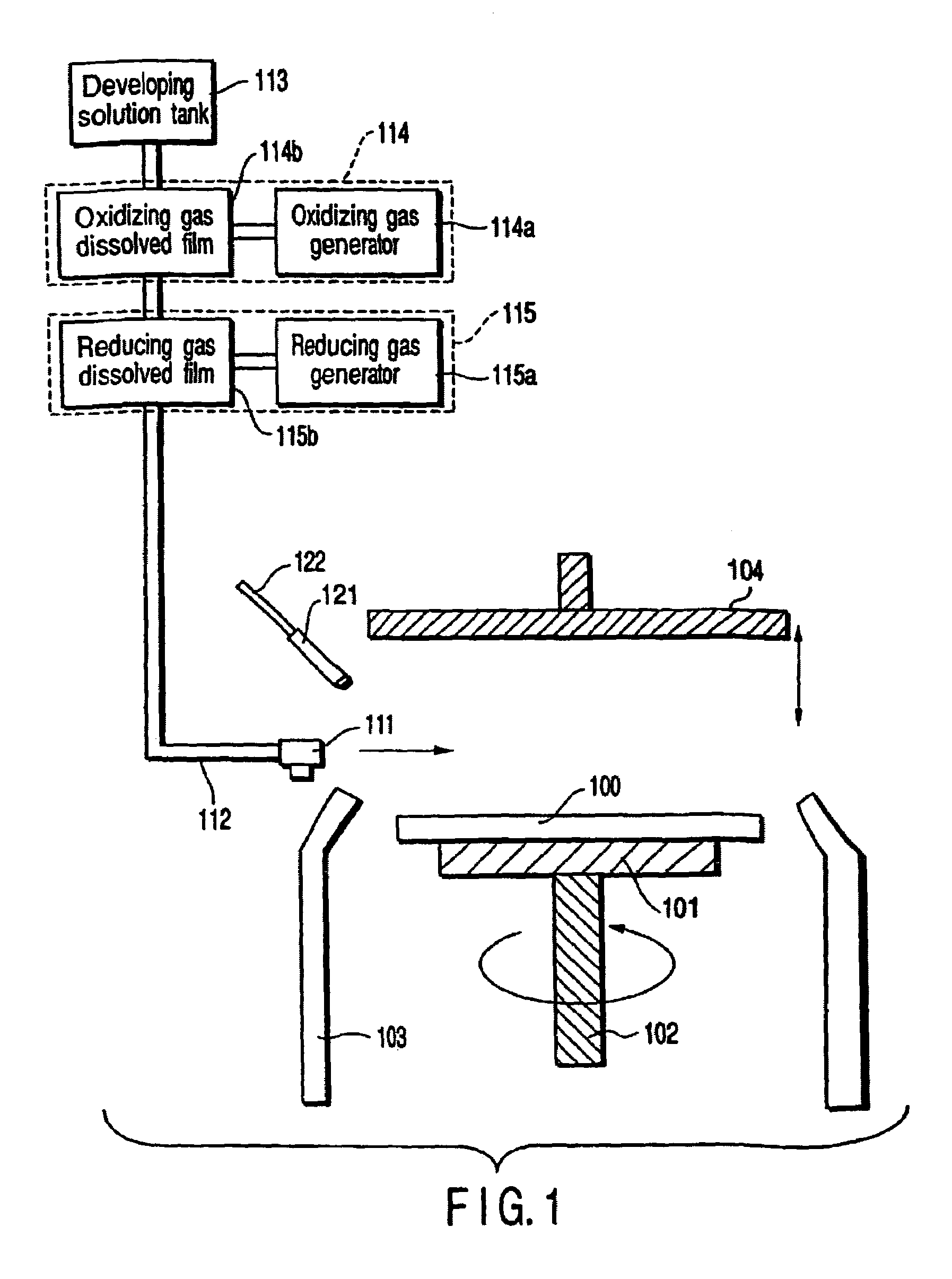
[0046](First Embodiment)

[0047]FIG. 1 is a diagram showing a schematic constitution of a developing unit according to a first embodiment of the present invention.

[0048]In the present unit, as shown in FIG. 1, a fixed base 101 onto which a substrate 100 is fixed is connected to a rotation mechanism 102 for rotating the fixed base 101 and substrate 100. A protective cup 103 with which the periphery of the substrate 100 is covered is disposed in order to prevent a developing solution, cleaning solution, and the like on the substrate 100 from being scattered during rotation of the substrate 100 by the rotation of the rotation mechanism 102.

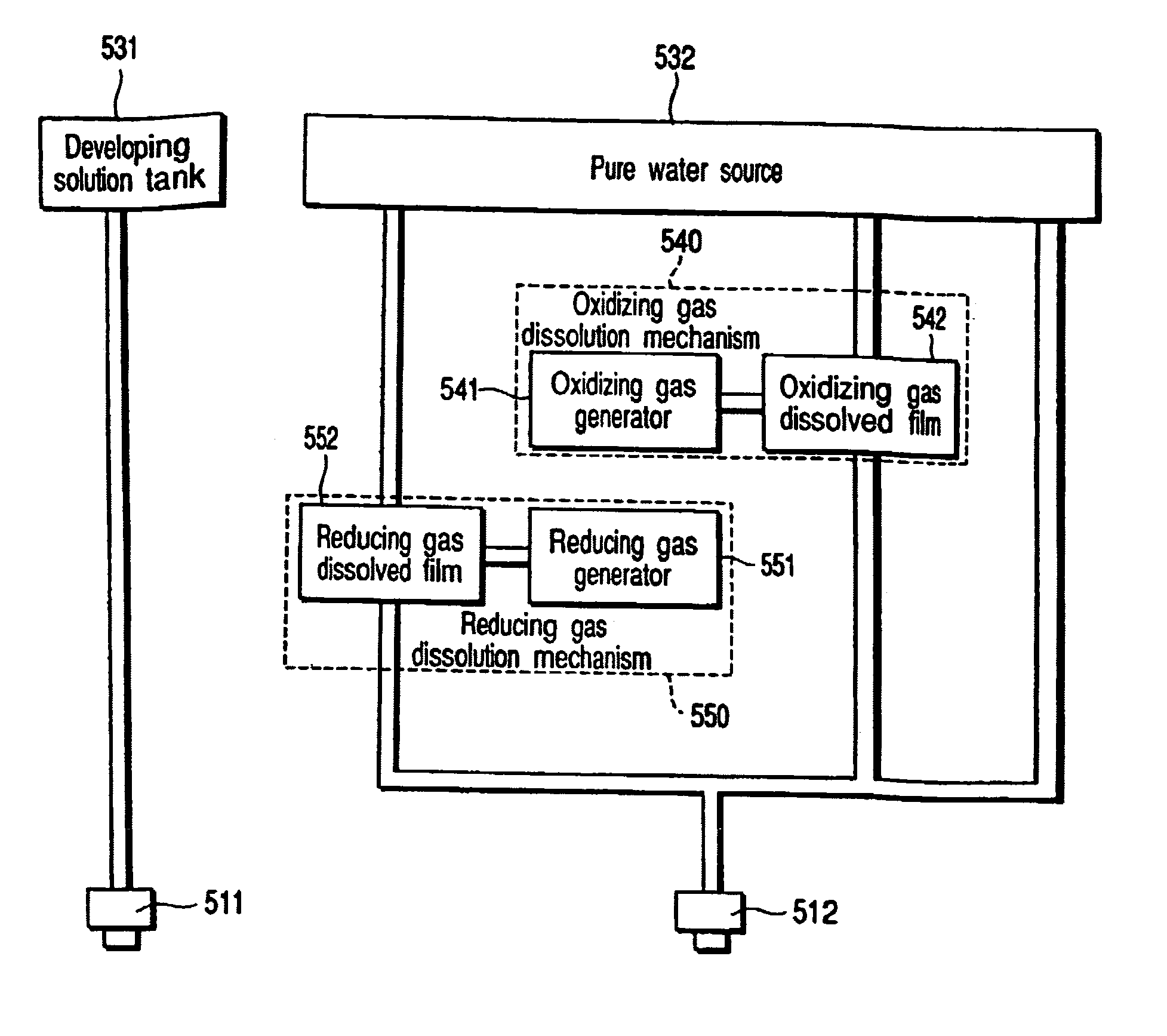
[0049]A developing solution supply nozzle 111 scanned on the substrate 100 is disposed. A developing tank 113 is connected to the developing solution supply nozzle 111 via a pipe 112. The deaerated developing solution is stored in the developing tank 113. The developing solution stored in the developing tank 113 is an aqueous solution such as alkaline ...

second embodiment

[0088](Second Embodiment)

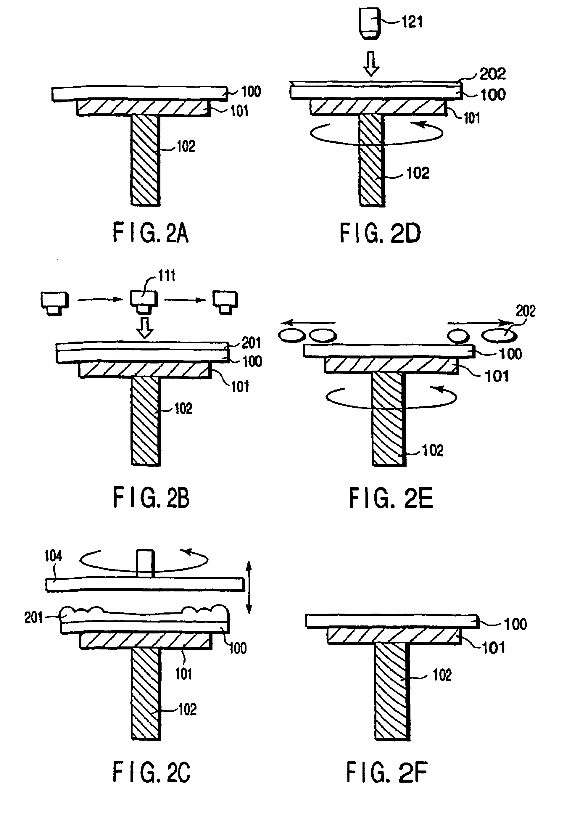
[0089]The developing method of supplying the reducing developing solution as the developing solution to the surface of the substrate by the developing unit shown in FIG. 1 will next be described with reference to FIGS. 4A to 4F. FIGS. 4A to 4F are process diagrams showing the developing process according to a second embodiment.

[0090]First, the substrate is coated with the anti-reflection coating, and chemically amplified resist, and the desired pattern is reduced projection exposure via the reticle for exposure by a KrF excimer laser. After the substrate is heat-treated (PEB), the substrate is conveyed to the developing unit, and held on the fixed base 101 (FIG. 4A).

[0091]Subsequently, the developing solution supply nozzle 111 is scanned from one end to the other end of the substrate 100, and the reducing developing solution is discharged in a curtain form so that a developing solution film 211 is formed on the substrate 100 (FIG. 4B). The developing solutio...

third embodiment

[0121](Third Embodiment)

[0122]FIG. 6 is a diagram showing a schematic constitution of a resist removing apparatus according to a third embodiment of the present invention.

[0123]As shown in FIG. 6, the present apparatus includes a treatment tank 301 in which an oxidizing remover 302 described later is stored. When a wafer cassette 300 with a plurality of substrates stored therein is immersed in the oxidizing removing solution 302, the resist on the substrate surface is removed.

[0124]The present apparatus further includes an oxidizing gas dissolution mechanism 310 for generating the oxidizing remover 302 stored in the treatment tank 301. The oxidizing gas dissolution mechanism 310 dissolves the oxidizing gas with respect to the deaerated removing solution stored in a removing solution tank 304, and generates the oxidizing removing solution 302. The generated oxidizing removing solution is supplied into the treatment tank 301 via a removing solution supply nozzle 303. The oxidizing gas...


PUM

PropertyMeasurementUnit
flow rateaaaaaaaaaa
timeaaaaaaaaaa
lengthaaaaaaaaaa

Abstract

A manufacturing method of an alkaline solution, comprising dissolving a gaseous molecule having oxidizing properties or reducing properties in an aqueous alkaline solution.

Description

CROSS-REFERENCE TO RELATED APPLICATIONS[0001]This application is a division of application Ser. No. 10 / 144,025, filed May 14, 2002, now U.S. Pat. No. 6,742,944 which is based upon and claims the benefit of priority from the prior Japanese Patent Application No. 2001-143682, filed May 14, 2001, all of which are incorporated herein by reference.BACKGROUND OF THE INVENTION[0002]1. Field of the Invention[0003]The present invention relates to a manufacturing method of an alkaline solution for developing and removing a resist film, and the like and the alkaline solution, a pattern forming method using the alkaline solution, a removing method of a resist film, a solution application apparatus, a substrate treatment method prior to forming the resist film, and a solution supplying method of scanning a linear solution supply nozzle from one end to the other end of a substrate, and supplying the solution onto the substrate from the solution supply nozzle to form a solution film on the substra...

Claims


Application Information

Patent Timeline
Patent Type & Authority Patents(United States)
IPC IPC(8): G03F7/32G03F7/30G03F7/38G03F7/40B01J19/00B05C5/02B05C11/10B05D1/26B05D3/00B05D3/10B05D7/00B05D7/24C02F1/68C09K3/00G03F7/42H01L21/027H01L21/311
CPCG03F7/3021G03F7/322H01L21/31133G03F7/425G03F7/422H01L21/027
Inventor TAKAHASHI, RIICHIROHAYASAKI, KEITAKEISHI, TOMOYUKIITO, SHINICHI
Owner KK TOSHIBA
Why Eureka
Try Eureka