

Multi-functional structure for enhanced chip manufacturibility and reliability for low k dielectrics semiconductors and a crackstop integrity screen and monitor
- Summary
- Abstract
- Description
- Claims
- Application Information
AI Technical Summary
Benefits of technology
Problems solved by technology
Method used
Image

Examples
Embodiment Construction
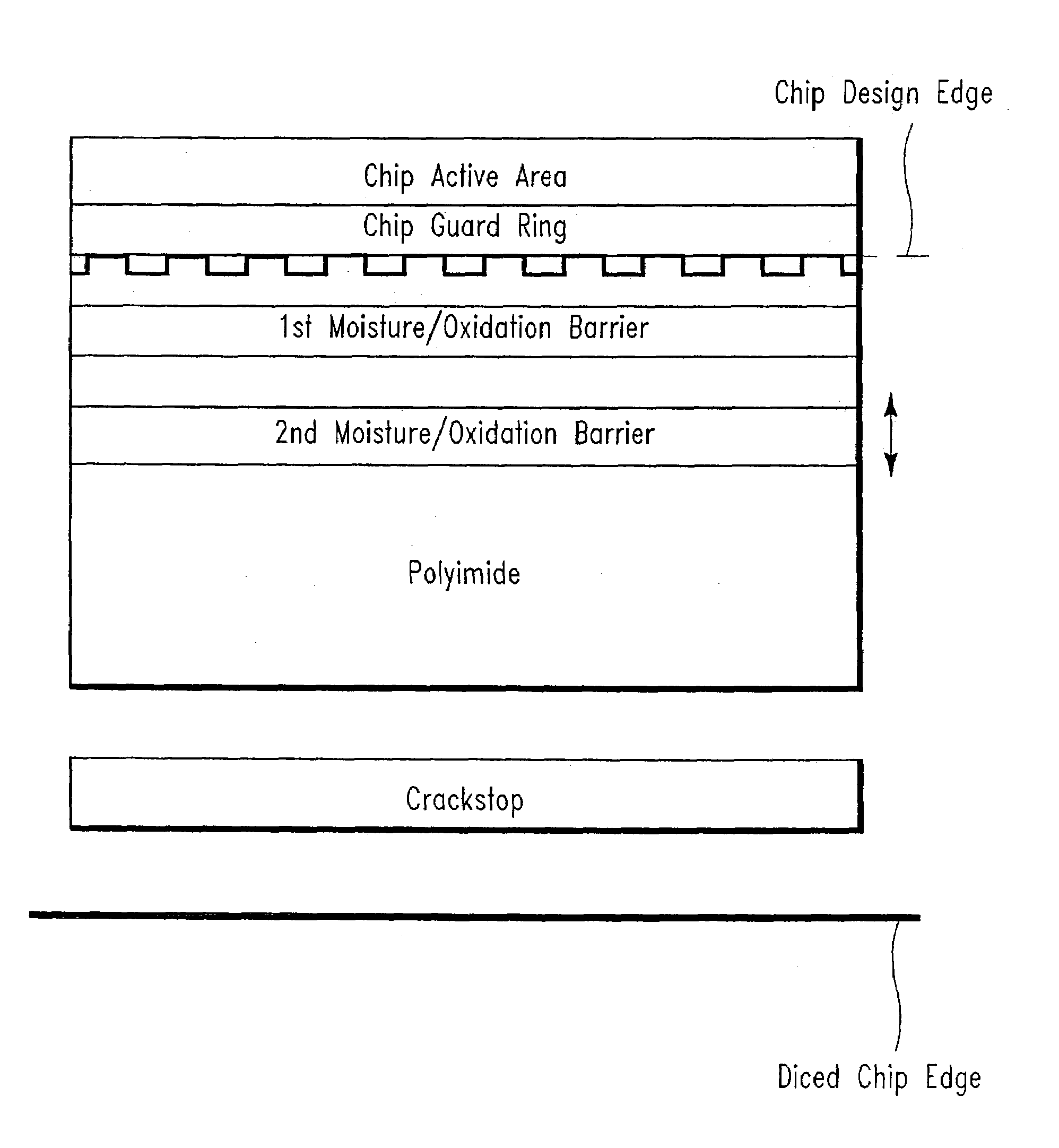
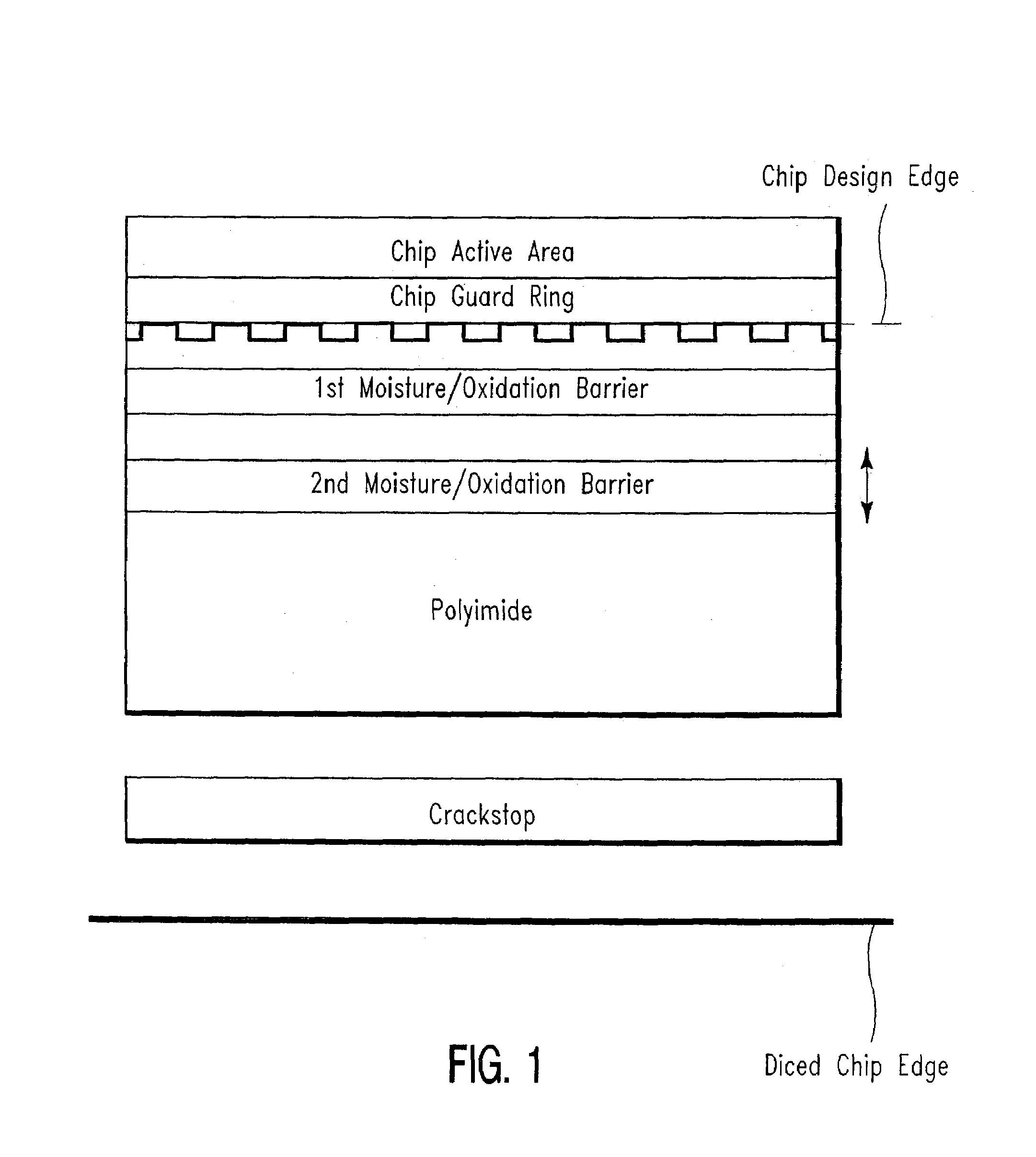
[0021]With reference to FIG. 1, there is illustrated an exemplary depiction of various barrier contours existing in the novel chip embodiment of the present invention. Beginning at a diced edge of an IC chip and moving inward toward a chip active circuit region, there is illustrated in sequence: a crackstop formed in the chip substrate, a polyimide layer typically on the chip's top surface, two oxidation / moisture barriers formed in the chip substrate, and, finally, a guard ring disposed adjacent to the chip's active circuit region, also formed in the chip substrate.
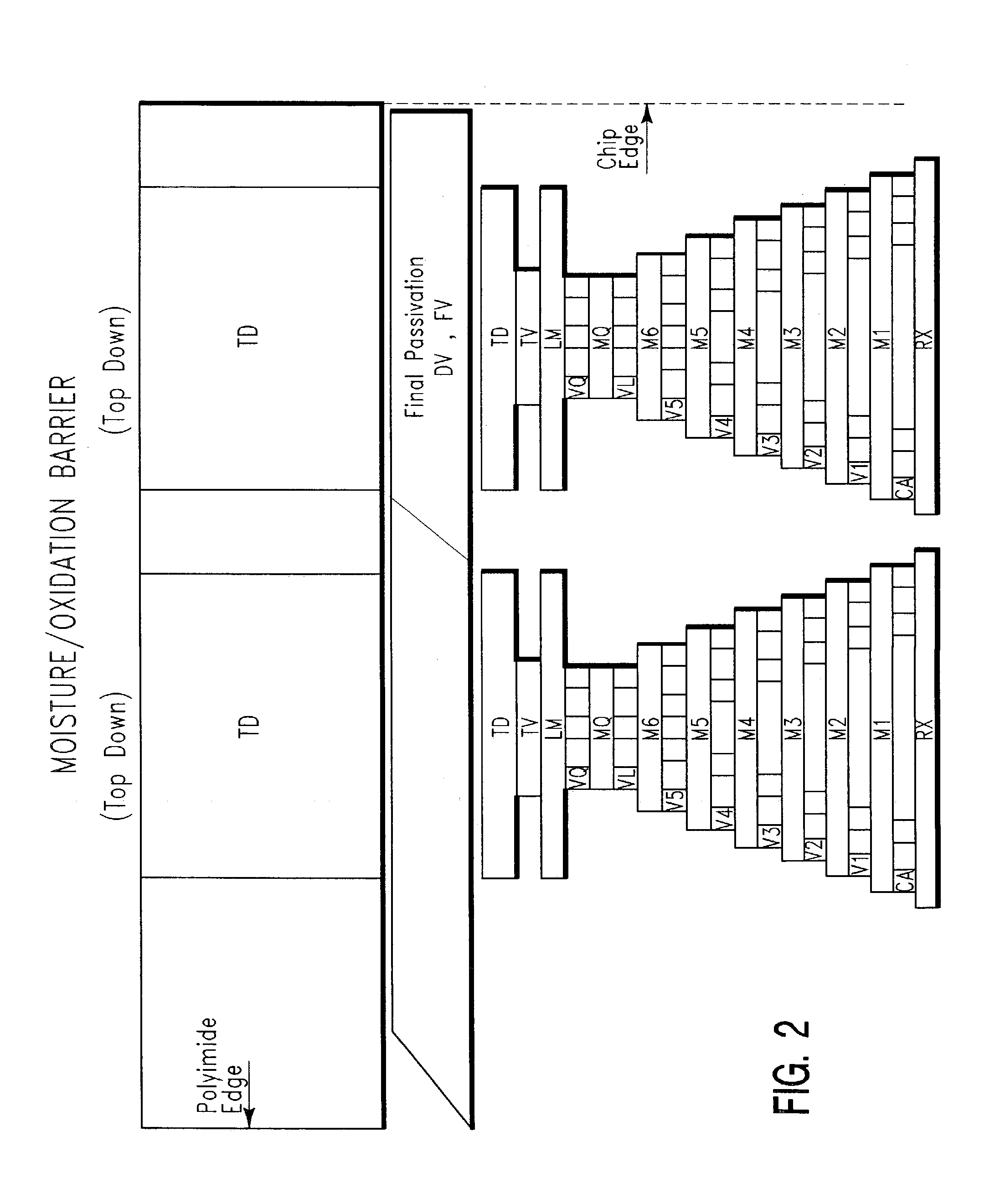
[0022]With reference to FIG. 2 (not drawn to scale), a top view is shown with a corresponding cross section view below. In the cross section view, there is illustrated the layered substrate structure of the fabricated barriers. Actual micrographs of the moisture / oxidatiaon barriers and mechanical crackstop are illustrated in FIGS. 11 and 12, respectively. The layers of the barriers include alternating layers of metal, lab...
PUM
 Abstract
Description
Claims
Application Information