Leadframe-based housing, leadframe strip, surface-mounted optoelectronic-component, and production method

a technology of leadframe and component housing, which is applied in the direction of semiconductor devices, electrical equipment, semiconductor/solid-state device details, etc., can solve the problems of reducing the overall height of components by reducing the height of the housing base body on the chip side, and increasing the risk of damage to components, etc., to achieve the effect of substantially reducing the overall height of components to be produced thereby

Active Publication Date: 2006-09-05
OSRAM OLED
View PDF13 Cites 75 Cited by
  • Summary
  • Abstract
  • Description
  • Claims
  • Application Information

AI Technical Summary

Benefits of technology

[0043]The particular advantage of the inventive production method resides in the fact that the overall height of a component housing to be produced thereby can be substantially reduced by means

Problems solved by technology

Such delamination would drastically increase the risk of damage to the component during further processing or later on during operation.
Current knowledge has it that the above-cited layer thickness of the injection compound must be so great that the mechanical tensile forces occurring in the injection compound during tear-off from the injection nozzle can be reduced to a level such that the forces exerted at the boundary with the leadframe are not sufficient to tear the injection compound away from the leadframe.
The possibility of reducing the overall height of components by decreasing the height of the

Method used


Image

  • Leadframe-based housing, leadframe strip, surface-mounted optoelectronic-component, and production method
  • Leadframe-based housing, leadframe strip, surface-mounted optoelectronic-component, and production method
  • Leadframe-based housing, leadframe strip, surface-mounted optoelectronic-component, and production method

Examples


Embodiment Construction

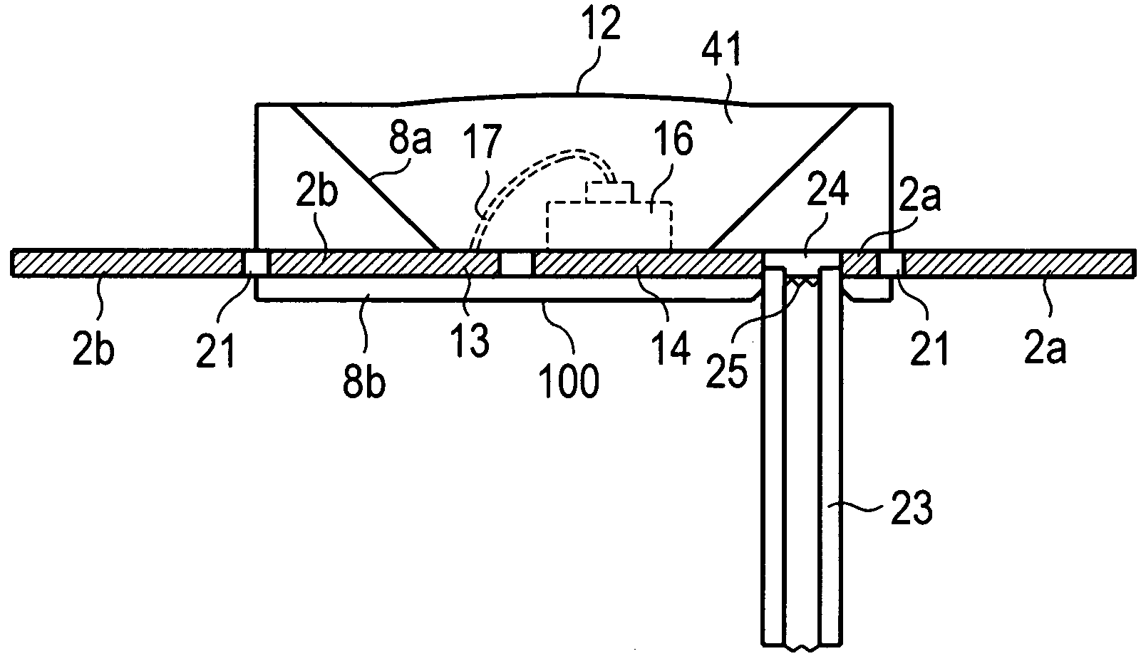
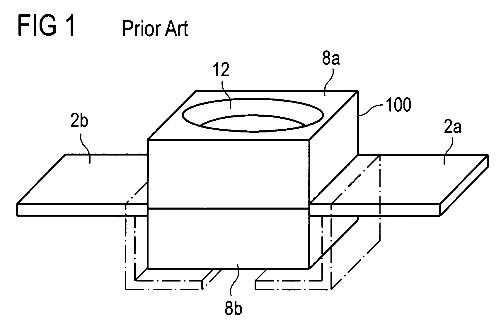
[0057]The housing base body of rectangular outline illustrated in FIG. 1 has a front portion 8a and a back wall 8b, a reflector recess comprising a radiation exit window 12 being provided in the front portion 8a. A first connector strip 2a and a second connector strip 2b are partially embedded in the housing base body and are connected to a radiation-emitting chip that is not shown here (it being hidden inside the housing base body). The projecting portions of the connector strips (external contacts) serve for contacting the component, e.g. to an external printed circuit board. The external contacts can extend perpendicularly to the corresponding side wall of the housing or, as indicated in broken lines in FIG. 1, they can be bent around the housing base body.

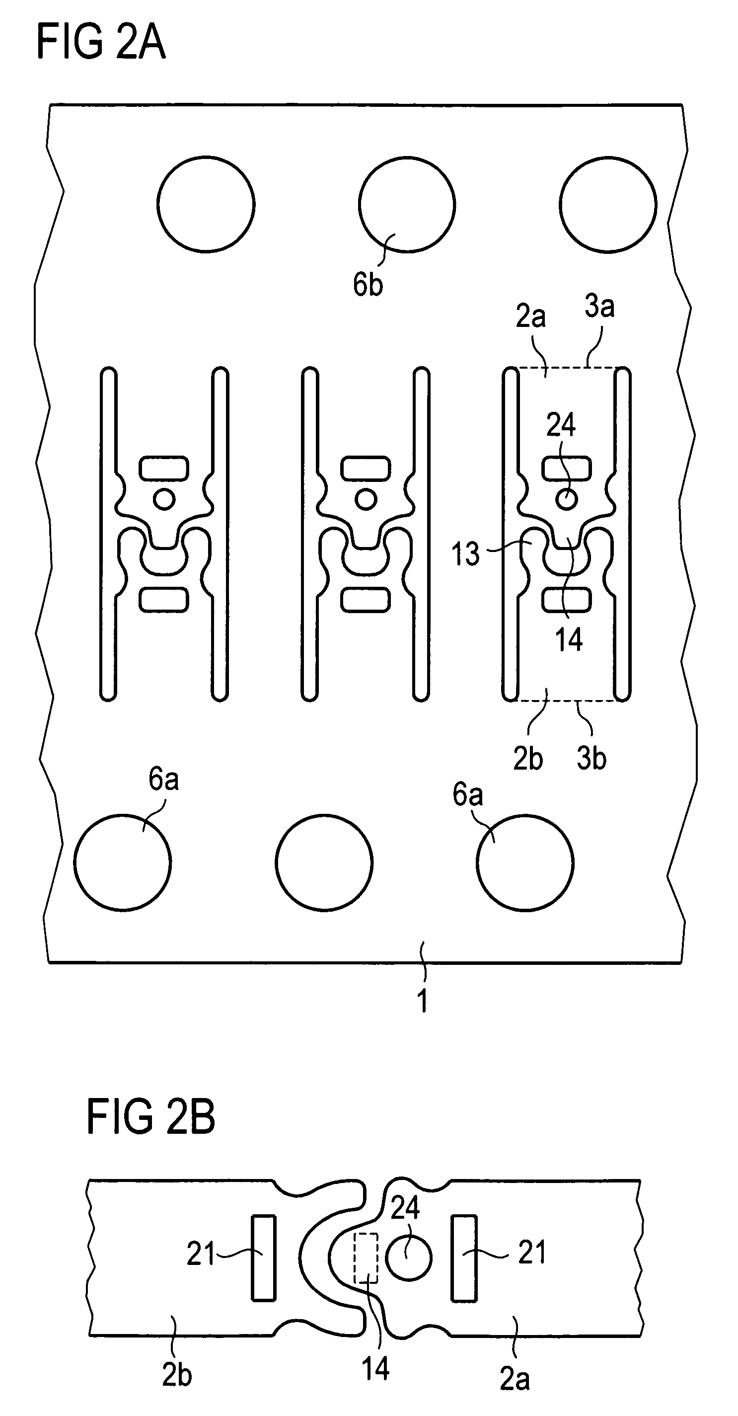
[0058]The leadframe ribbon 1 according to the embodiment example of FIGS. 2a and 2b is prestructured, for example by stamping, and comprises in particular a plurality of first connector strips 2a and a plurality of second conne...


PUM


Abstract

A leadframe-based housing for a surface-mountable component, particularly a radiation-emitting component. The leadframe-based housing comprises electrical connector strips and at least one chip mounting area. One of the connector strips includes an injection aperture that enables a leadframe-based housing to be produced with a very small thickness in an injection molding process. A method for producing such housings is further specified.

Description

CROSS-REFERENCE TO RELATED APPLICATIONS[0001]This application is the National Stage of International Application No. PCT / DE2003 / 001906, filed Jun. 10, 2003, which claims the benefit of German Patent Application Serial No. 10234704.2, filed on Jul. 30, 2002. The contents of both applications are hereby incorporated by reference in their entireties.FIELD OF THE INVENTION[0002]The invention concerns a leadframe-based component housing, a leadframe ribbon with pre-injection-molded component housings, a surface-mountable electronic component, particularly a component comprising a radiation-emitting or radiation-detecting chip, for example a light-emitting diode, also known as an LED, and the method for producing said leadframe-based component housing.BACKGROUND OF THE INVENTION[0003]The invention concerns electroluminescent diode components suitable in particular for surface-mounting on a printed circuit board, in which a housing base body produced by injection molding and comprising par...

Claims


Application Information

Patent Timeline
IPC IPC(8): H01L23/495H01L23/043H01L23/24H01L31/02H01L33/48H01L33/62
CPCH01L31/0203H01L33/486H01L33/62H01L2224/48091H01L2224/48247H01L2924/12041H01L2924/0102H01L2924/01078H01L2924/01004H01L2924/00014
Inventor SORG, JORG ERICH
Owner OSRAM OLED
Why Eureka
Try Eureka