Stacked memory, memory module and memory system

a memory module and memory technology, applied in the field of stacking memory, can solve the problems of short distance between wirings, inability to meet the needs of users, and memory performance to be degraded, and achieve the effect of low power consumption and high speed data transmission

Inactive Publication Date: 2006-09-05
LONGITUDE SEMICON S A R L
View PDF10 Cites 101 Cited by
  • Summary
  • Abstract
  • Description
  • Claims
  • Application Information

AI Technical Summary

Benefits of technology

[0023]It is an object of the present invention to provide a memory module of a four-rank configuration that allows a high speed data transmission without degrading a signal quality and also allows coordinating the transmission characteristics of signal wirings of a variety of control signals, and further that is advantageous for realizing low power consumption.
[0025]In the above stacked memories, it is not required that neighboring memories share a point-to-point bus (DQ signal wirings) when the stacked memories are employed for a memory module in a four-rank configuration, because a plurality of memory chips built in each stacked memory share a signal terminal. Accordingly, it is avoided to branch the DQ signal wiring or impose a limitation on the DQ signal wiring in the wiring direction.
[0027]This construction makes it possible to increase the area of the wiring region of the point-to-point bus, reserve the spacing between the DQ signal wirings, and equalize the lengths of the DQ signal wirings, because the stacked memories are arranged on the module substrate spaced apart by a distance equivalent to the length of one stacked memory. Consequently, the cross-talk noise and ISI (Intersignal interference) noise of the DQ signals and the variations in the arrival timings of the signals are suppressed.
[0029]Particularly, the performance of the simultaneous selection of the memory chips included in the stacked memories mounted on one surface of the module substrate alternately with the simultaneous selection of the memory chips included in the stacked memories mounted on another surface of the module substrate causes the heat generated in the memory chips to distribute over both surfaces of the memory module, thereby entailing an enhancement of the efficiency of the heat dissipation to mitigate a temperature rise in the memory chip, whereby the degradation of the memory characteristics is suppressed.

Problems solved by technology

Nevertheless, a problem has been known concerning a memory module that the speed-up of memory access generally entails an increase in power consumption, which in turn causes the temperature of a package to be raised and consequently the performance of a memory to be degraded.
However, memories are mounted on a module substrate nearly too closely to leave any room so that distances between wirings are short and also limitations are imposed on the wiring directions of the DQ signal wirings for memories.
Consequently, the degree of wiring freedom of the DQ signal wiring markedly drops down, the wiring lengths connecting to two memories become asymmetric and significantly fluctuate, and cross-talk noise and ISI (intersignal interference) noise increase.
Furthermore, the fluctuations in the arrival timings of signals increase, the qualities of waveforms of the DQ signals are degraded causing difficulty in a high-speed transmission through a bus.

Method used


Image

  • Stacked memory, memory module and memory system
  • Stacked memory, memory module and memory system
  • Stacked memory, memory module and memory system

Examples


first embodiment

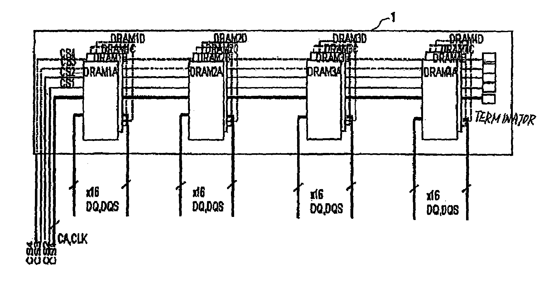
[0068]A memory module of a first embodiment is configured such that stacked memories are employed for memories to be mounted on a module substrate with two memories (memory chips) sharing signal terminals and the spacing between the stacked memories is widened to allow the degree of freedom in a DQ signal wiring to be ensured.

[0069]As shown in FIGS. 3A and 3B, memory module 1 of the first embodiment is mounted with sixteen memory chips and configured to have four ranks with 64-bit I / O. Memory module 1 is mounted with a total of eight stack memories 3, four stack memories 3 being mounted on each of the front and reverse surfaces of module substrate 2, wherein each stack memory 3 has a plurality of built-in memory chips (two memory chips in FIGS. 3A, 3B). Accordingly, the number of the memory chips amounts to sixteen. Each stacked memory 3 is provided with 16-bit I / O and each of the two memory chips incorporated in stacked memory 3 is also adapted for 16-bit I / O. The two memory chips ...

second embodiment

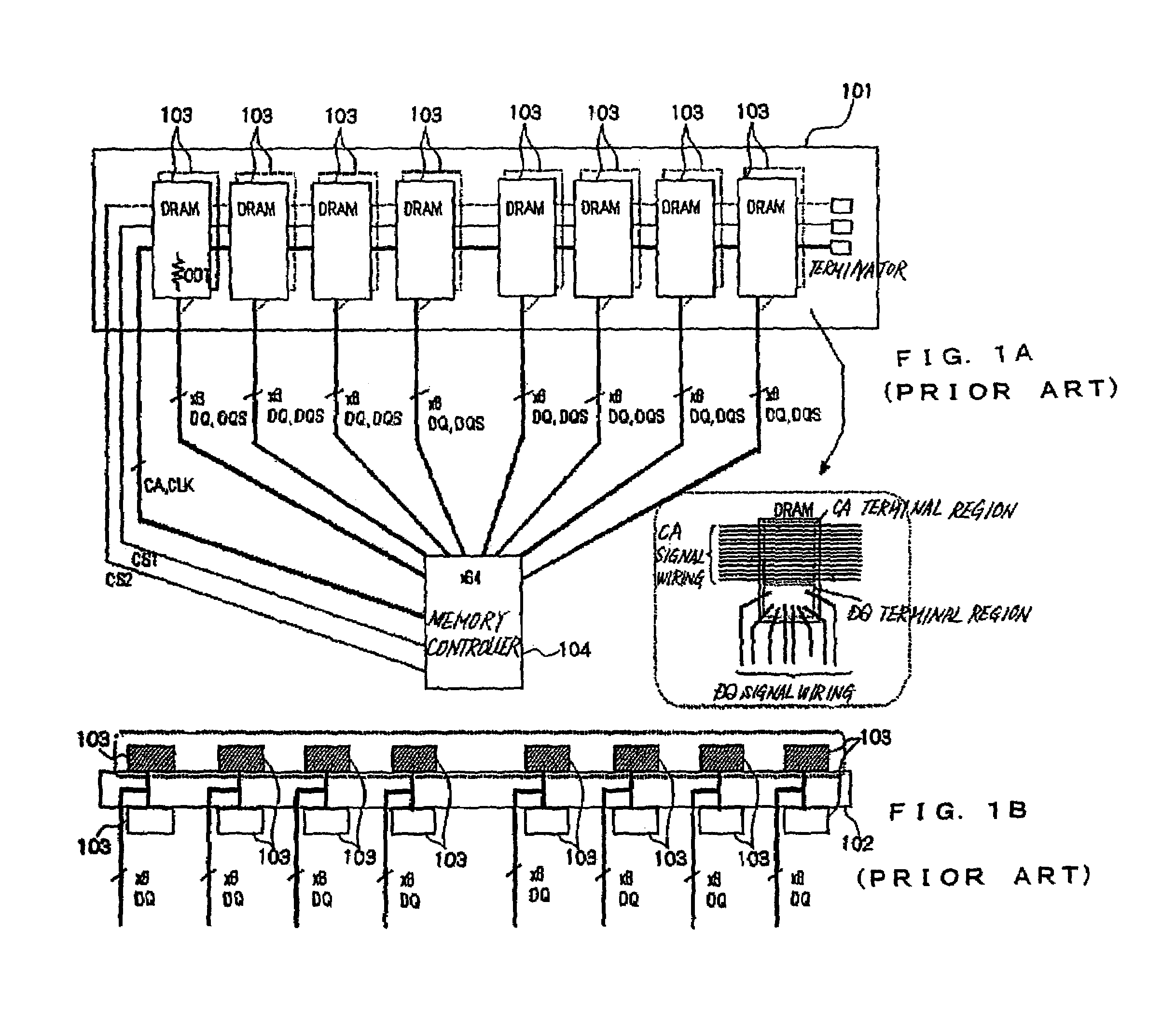
[0079]In the memory module of the first embodiment, if an ordinary stacked memory as shown in FIG. 5A is employed as a stacked memory for mounting on a memory module, a load capacitance equivalent to four memories are connected to the daisy chain bus at prescribed intervals. Consequently, the characteristic impedance of the transmission line locally varies significantly so that a waveform of a signal carried by the daisy chain bus, such as the CA signal, might be deteriorated.

[0080]Stacked memory 300 shown in FIG. 5A is configured such that first memory chip 302 is mounted face down (with chip pad 309 directed downward) on package substrate 301 having BGA (BAII Grid Array: a group of ball terminals 305 arranged in an array) on the bottom face and second memory chip 303 is mounted face up (with chip pad 309 directed upward) on first memory chip 302 and fixed with sealing material 304.

[0081]Package substrate 301 has, for example, power-supply / GND (ground potential) layer 306 formed on...

third embodiment

[0103]As shown in FIG. 11, stacked memory 23 of a third embodiment is configured such that four memories 402 each provided with through holes 408 are mounted on package substrate (interposer) 401 having ball terminals (signal terminals) 405 for electrically connecting with the module substrate. A technology of stacking a plurality of memory chips on a interposer 401 as described above is called CoC (Chip-on-Chip), wherein each memory chip 402 and ball terminal 405 are electrically connected through via through holes 408 bored through memory chips 402 and signal wirings formed in interposer 401.

[0104]For reference, the CoC technology is explained in detail, for example, Y. Akiyama et al., “Superfine Pitch Ultrasonic Bonding Technology on 3D Stacked LSI”, ICEP (International Conferences of Electronics Packaging) Proceedings, pp. 326–331, 2003., or K. Takahashi et al., “Current Status of Research and Development for 3D Chip Stack Technology” Jpn. J. Appl. Phys., Vol. 40(4B), pp. 3032, ...


PUM


Abstract

A point-to-point bus and a daisy chain bus are provided for supplying signals to stacked memories, and the stacked memories are mounted mutually apart by a distance equivalent to the length of the stacked memory on both surfaces of a module substrate. Furthermore, the memory chips arranged in a stacked memory mounted on one surface are set in an active state at the same time alternately with the memory chips arranged in a stacked memory mounted on another surface of the module substrate.

Description

BACKGROUND OF THE INVENTION[0001]1. Field of Invention[0002]The present invention relates to a stacked memory having a plurality of built-in memory chips, a memory module mounted with a plurality of stacked memories and a memory system having the memory module.[0003]2. Description of the Related Art[0004]An access time of a memory such as a DRAM has recently been sped up and with this, memory systems making use of a point-to-point bus and a daisy chain bus have come to be an object for consideration in order to ensure the waveform quality of signals transmitted at high speeds (cf., for example, RAMBUS Co. U.S.A., Yellowstone Memory System: Rich Warmke, “Yellowstone, A Next Generation memory Signaling Technology” RAMBUS DEVELOPER FORUM, OCT. 29, 2002, [Oct. 30, 2003, retrieved] internet <URL:[0005]http:rambus.com / rdf / rdf2002 / pdf / rdf_consumer_track.pdf.>)[0006]More specifically, memory modules have been envisioned which use multibit point-to-point buses to transmit DQ (data) sig...

Claims


Application Information

Patent Timeline
Patent Type & Authority Patents(United States)
IPC IPC(8): G11C5/02G11C7/00G06F12/00G06F13/16G11C5/00G11C5/04G11C11/401H01L25/065H01L25/10H01L27/10H05K1/18
CPCG11C5/04H01L25/0652H01L25/105H05K1/181H01L25/0657H01L2924/13091H01L2225/06541H01L2225/06513H01L2924/3011H05K2201/10159H05K2201/10515H05K2203/1572H01L2924/15311H01L2924/15321H01L2225/06565H01L2224/48091H01L2224/48227H01L2224/73265H01L2225/1023H01L2225/107H01L2225/1005H01L2225/06517H01L2924/00014H01L2924/00Y02P70/50
Inventor FUNABA, SEIJINISHIO, YOJI
Owner LONGITUDE SEMICON S A R L
Why Eureka
Try Eureka