Active-matrix substrate and electromagnetic wave detector

a technology of active matrix which is applied in the field of active matrix substrate and electromagnetic wave detector, can solve the problems of reducing the sensitivity of the electromagnetic wave detector, reducing the proportional decrease in the area occupied by poor efficiency of collecting charge, so as to maximize the fill factor of the charge collecting electrode, the effect of improving the s/n ratio

Active Publication Date: 2006-09-26
SHARP KK +1
View PDF4 Cites 0 Cited by
  • Summary
  • Abstract
  • Description
  • Claims
  • Application Information

AI Technical Summary

Benefits of technology

[0013]An object of the present invention is to provide a large-area and high-resolution electromagnetic wave detector having an improved S / N ratio, using an active-matrix array that can maximize the fill factor of the charge collecting electrodes.

Problems solved by technology

A drawback of such a pixel layout, however, is that the increased gap between the charge collecting electrodes 103 and the scanning and signal lines 107 and 108 brings about a proportional decrease in the area occupied by the charge collecting electrodes 103 (also known as and hereinafter referred to as “fill factor”).
With the reduced fill factor of the charge collecting electrodes 103, the efficiency of collecting charge becomes poor, and the sensitivity of the electromagnetic wave detector drops.

Method used


Image

  • Active-matrix substrate and electromagnetic wave detector
  • Active-matrix substrate and electromagnetic wave detector
  • Active-matrix substrate and electromagnetic wave detector

Examples


first embodiment

[0028][First Embodiment]

[0029]One embodiment of the present invention is described below with reference to the attached drawings. As used herein, the term “electromagnetic wave detector” refers to an electromagnetic wave detector with a two-dimensional array of electromagnetic wave detecting elements respectively corresponding to the pixels of a detected image.

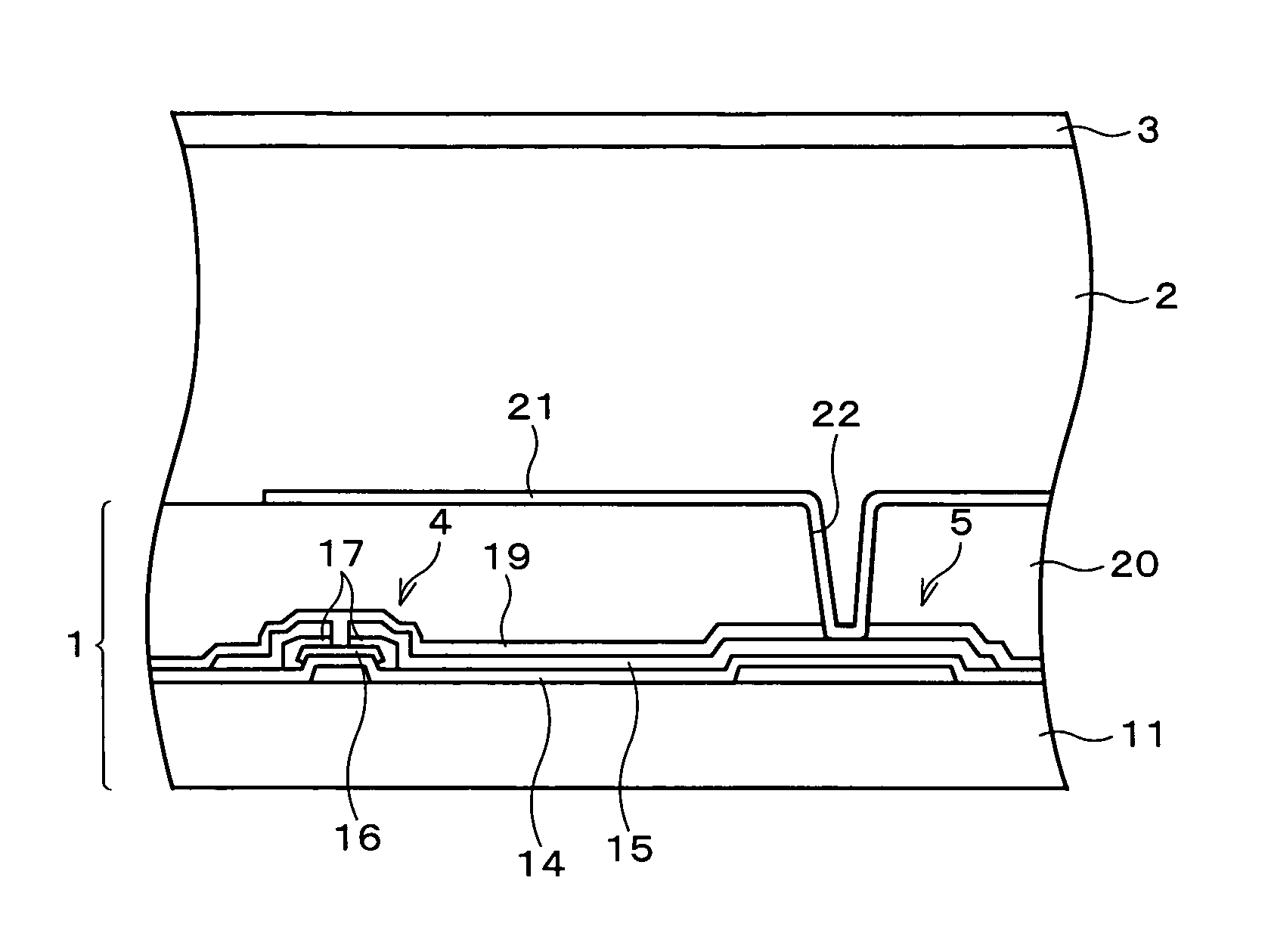
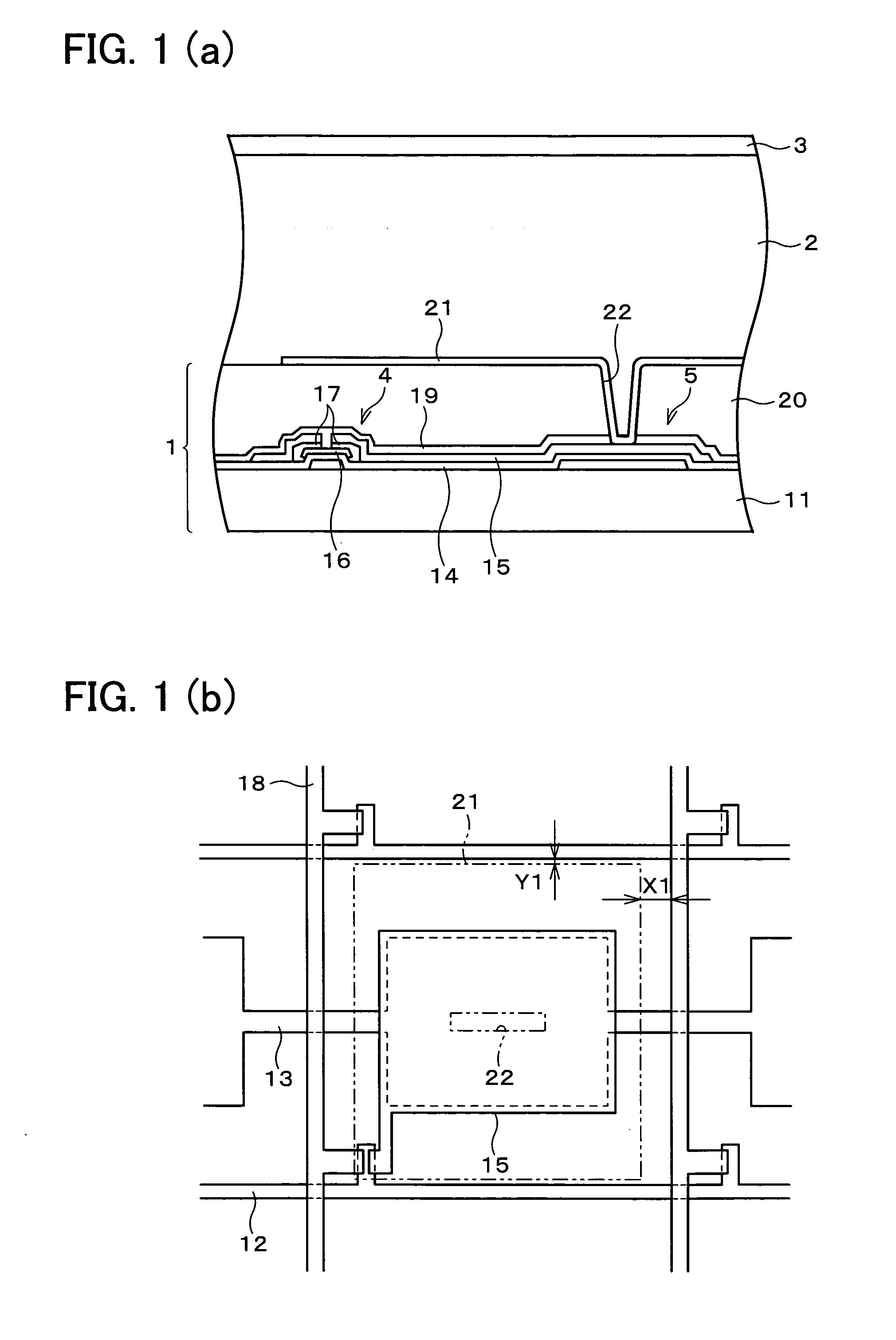
[0030]FIG. 1(a) is a plan view illustrating a pixel-wise structure of the electromagnetic wave detector, and FIG. 1(b) is a cross sectional view of the structure shown in FIG. 1(a). The pixel illustrated in FIG. 1(a) and FIG. 1(b) measures about 0.1 mm×0.1 mm to about 0.3 mm×0.3 mm, and the electromagnetic wave detector generally includes about 500×500 to about 3000×3000 pixels of this size that are disposed in an X-Y matrix. For the radiography of the chest, the electromagnetic wave detector should measure about 17×17 inches.

[0031]As illustrated in FIG. 1 (a) and FIG. 1 (b), the electromagnetic wave detector includes an activ...

second embodiment

[0060][Second Embodiment]

[0061]Referring to the attached drawings, the following will describe a modification example of the electromagnetic wave detector of the First Embodiment.

[0062]FIG. 3 is a plan view illustrating a pixel-wise structure of an electromagnetic wave detector of the present embodiment. As to the cross sectional structure, the electromagnetic wave detector of the present embodiment is basically the same as that described in the First Embodiment.

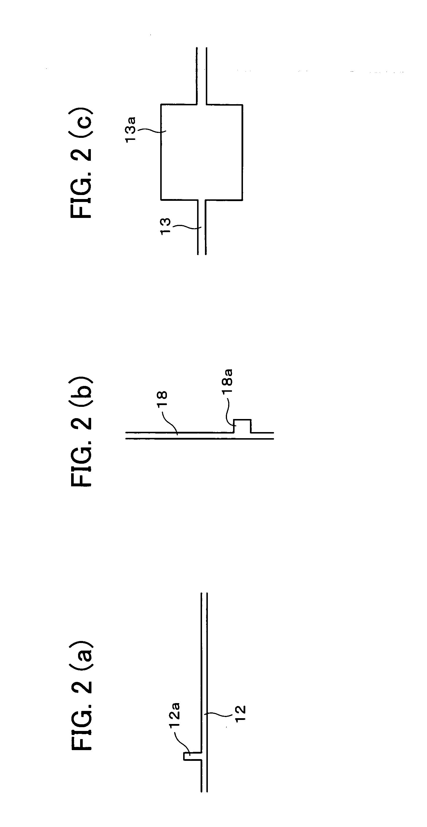
[0063]The present embodiment has a pixel layout that differs from the First Embodiment with respect to the profile of the capacitor electrodes 13a defining the capacitors 5. Specifically, as illustrated in FIG. 3, a relation X2>Y2 is satisfied, where X2 is the gap between the capacitor electrodes 13a and the signal lines 18, and Y2 is the gap between the capacitor electrodes 13a and the scanning lines 12.

[0064]The advantages of the layout shown in FIG. 3 are described below. As illustrated in FIG. 4, in the pixel layout show...


PUM


Abstract

Pixel electrodes on an active-matrix substrate do not overlap signal lines and scanning lines, and satisfy a relation X1>Y1, where X1 is the gap between the pixel electrodes and the signal lines, and Y1 is the gap between the pixel electrodes and the scanning lines. As a result, a large-area and high-resolution electromagnetic wave detector is realized with an improved S/N ratio, even with an active-matrix array providing a large area for the charge collecting electrodes.

Description

[0001]This Nonprovisional application claims priority under 35 U.S.C. § 119(a) on Patent Application No. 2003 / 016754 filed in Japan on Jan. 24, 2003, the entire contents of which are hereby incorporated by reference.FIELD OF THE INVENTION[0002]The present invention relates to electromagnetic wave detectors for detecting an image of electromagnetic waves including X-ray radiation, visible light, and infrared light. The invention also relates to a structure of an active-matrix substrate used therefor.BACKGROUND OF THE INVENTION[0003]In one conventional example of an electromagnetic wave detector, charge collecting electrodes for collecting generated charges in a semiconductor film are two-dimensionally disposed in rows and columns over the semiconductor film, and a switching element is provided for each pixel of the array. The semiconductor film is provided as an electromagnetically conductive film (also known as a photoconductive film) for generating charges (electron-hole pairs) by ...

Claims


Application Information

Patent Timeline
Patent Type & Authority Patents(United States)
IPC IPC(8): H01L31/00H01L27/146G01R29/08G01T1/16H01L21/77H01L27/12H01L27/13H01L27/14H01L29/786H04N5/335H04N5/357H04N5/369H04N5/374
CPCH01L27/14658H01L27/124H01L27/1255E03C1/01E03D1/003E03D1/263E03D1/304E03D1/33E03D5/003
Inventor IZUMI, YOSHIHIROSATO, KENJI
Owner SHARP KK
Why Eureka
Try Eureka