

Image sensor and method for manufacturing the sensor
An image sensor, conductive type technology, applied in semiconductor/solid-state device manufacturing, electric solid-state devices, semiconductor devices, etc., can solve the problems of output image sensitivity drop, image error, dark current saturation and sensitivity, etc., to minimize saturation decrease in accuracy and sensitivity, maximize fill factor, and minimize charge-sharing effects
Inactive Publication Date: 2010-12-01
DONGBU HITEK CO LTD
View PDF0 Cites 0 Cited by
- Summary
- Abstract
- Description
- Claims
- Application Information
AI Technical Summary
Problems solved by technology
When the charge sharing phenomenon occurs, the sensitivity of the output image decreases and image errors occur
Also, because photocharges may not move easily between the photodiode and the readout circuitry, dark currents can be generated and / or saturation and sensitivity degraded
Method used
View moreImage
Smart ImageViewing Examples

Examples
Embodiment Construction
Login to View More PUM
 Abstract
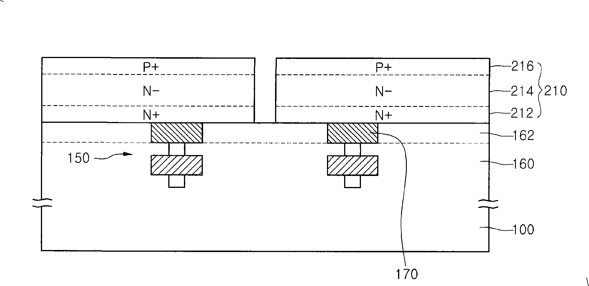
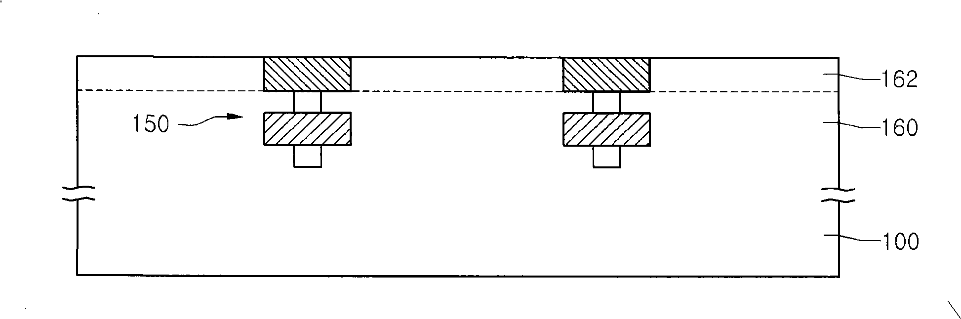
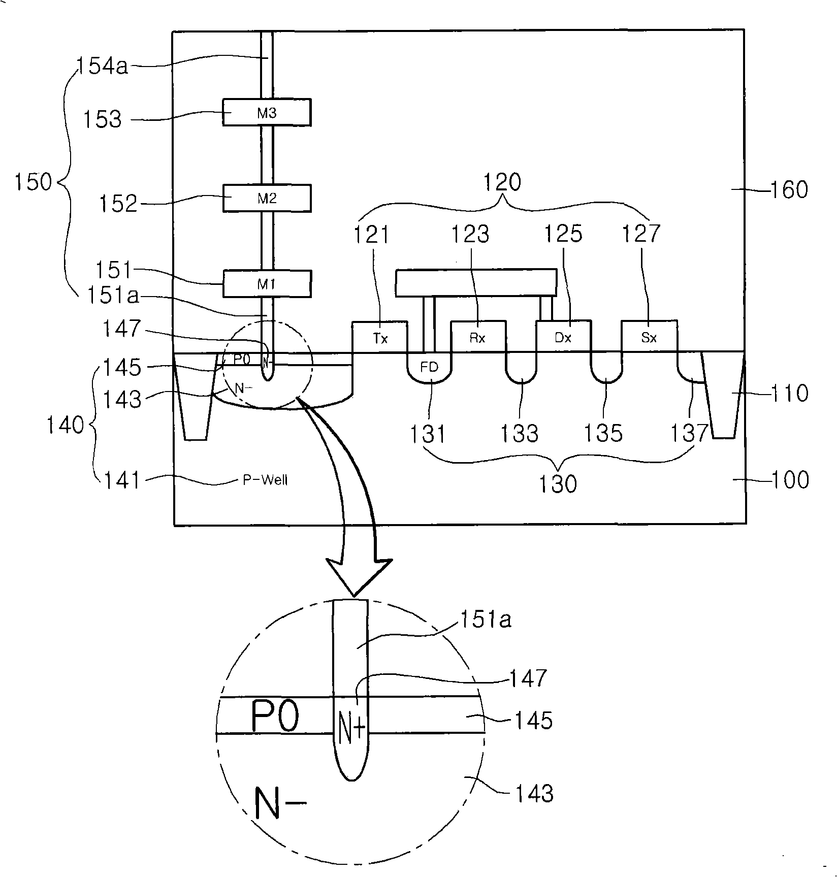
An image sensor includes a readout circuitry, a first substrate, a first interlayer dielectric, a metal interconnection, a top metal, and an image sensing device. The readout circuitry is formed on and / or over the first substrate and the first interlayer dielectric is formed on and / or over the first substrate. The metal interconnection is formed in the interlayer dielectric and electrically connected to the readout circuitry. The top metal is formed on and / or over the metal interconnection and the image sensing device is formed on and / or over the top metal. The disclosed manufacturing method of the image sensor can maximize a physical and electrical bonding force between an image sensing device and a metal interconnection, minimize the occurrence of charge sharing while maximizing a fill factor, and minimize a dark current source and minimize reduction in saturation and sensitivity.
Description
Image sensor and manufacturing method thereof technical field The invention relates to an image sensor and a manufacturing method thereof. Background technique An image sensor is a semiconductor device that converts an optical image into an electrical signal. Image sensors may generally be classified as Charge Coupled Device (CCD) image sensors or Complementary Metal Oxide Semiconductor (CMOS) image sensors (CIS). During the fabrication of image sensors, ion implantation may be used to form photodiodes in the substrate. In order to increase the number of pixels without increasing the size of the chip, the size of the photodiode has been continuously reduced, thereby also reducing the area of the light receiving portion, resulting in a decrease in image quality. However, since the stack height is not reduced to the extent that the light receiving part is reduced, photons incident on the light receiving part due to light diffraction (known as "ariydisk") amount will de...
Claims
Login to View More Application Information
Patent Timeline
 Patent Type & AuthorityPatents(China)
IPC IPC(8): H01L27/146H01L23/522H01L21/822H01L21/768
CPCH01L27/14612H01L27/14632H01L27/14634H01L27/14636H01L27/14687
Inventor张贞烈玄祐硕
OwnerDONGBU HITEK CO LTD