Smooth fin topology in a FinFET device

a finfet and smooth technology, applied in the field of double gate devices, can solve the problems of increasing difficulty in overcoming, short channel effects, excessive leakage between the source and drain, etc., and achieve the effect of improving the topology and reducing the effect of “micromasking”

Inactive Publication Date: 2006-09-26
ADVANCED MICRO DEVICES INC
View PDF7 Cites 7 Cited by
  • Summary
  • Abstract
  • Description
  • Claims
  • Application Information

AI Technical Summary

Benefits of technology

[0006]Implementations consistent with the present invention provide a double-gate MOSFET having an improved topology in the gate area. The improved topology can lead to reduced “micromasking” effects that may otherwise be encountered during patterning / etching of the gate.

Problems solved by technology

The reduction of design features below 100 nm challenges the limitations of conventional methodology.
For example, when the gate length of conventional planar metal oxide semiconductor field effect transistors (MOSFETs) is scaled below 100 nm, problems associated with short channel effects, such as excessive leakage between the source and drain, become increasingly difficult to overcome.
In addition, mobility degradation and a number of process issues also make it difficult to scale conventional MOSFETs to include increasingly smaller device features.

Method used


Image

  • Smooth fin topology in a FinFET device
  • Smooth fin topology in a FinFET device
  • Smooth fin topology in a FinFET device

Examples


Embodiment Construction

[0019]The following detailed description of the invention refers to the accompanying drawings. The same reference numbers may be used in different drawings to identify the same or similar elements. Also, the following detailed description does not limit the invention. Instead, the scope of the invention is defined by the appended claims and equivalents.

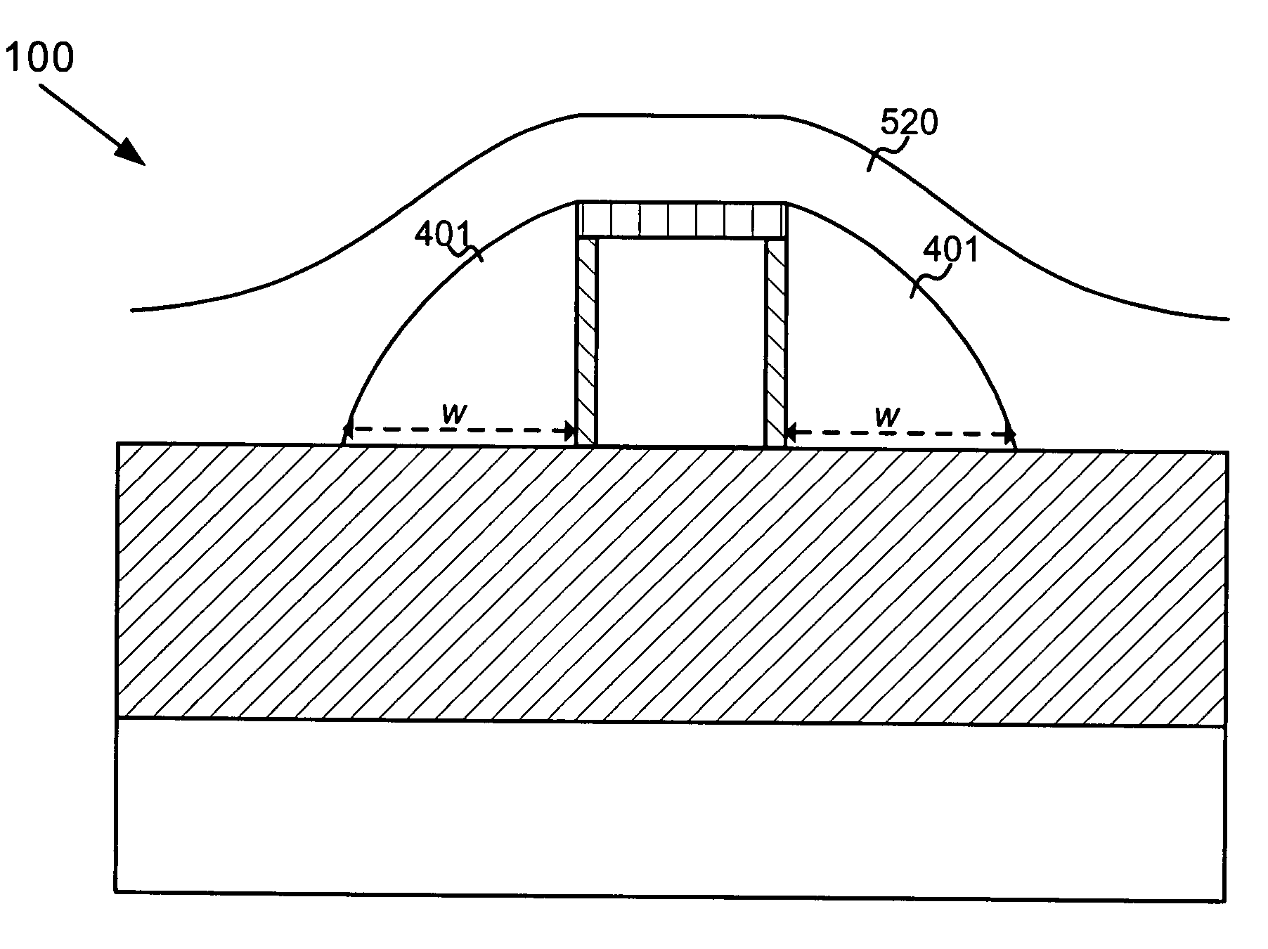
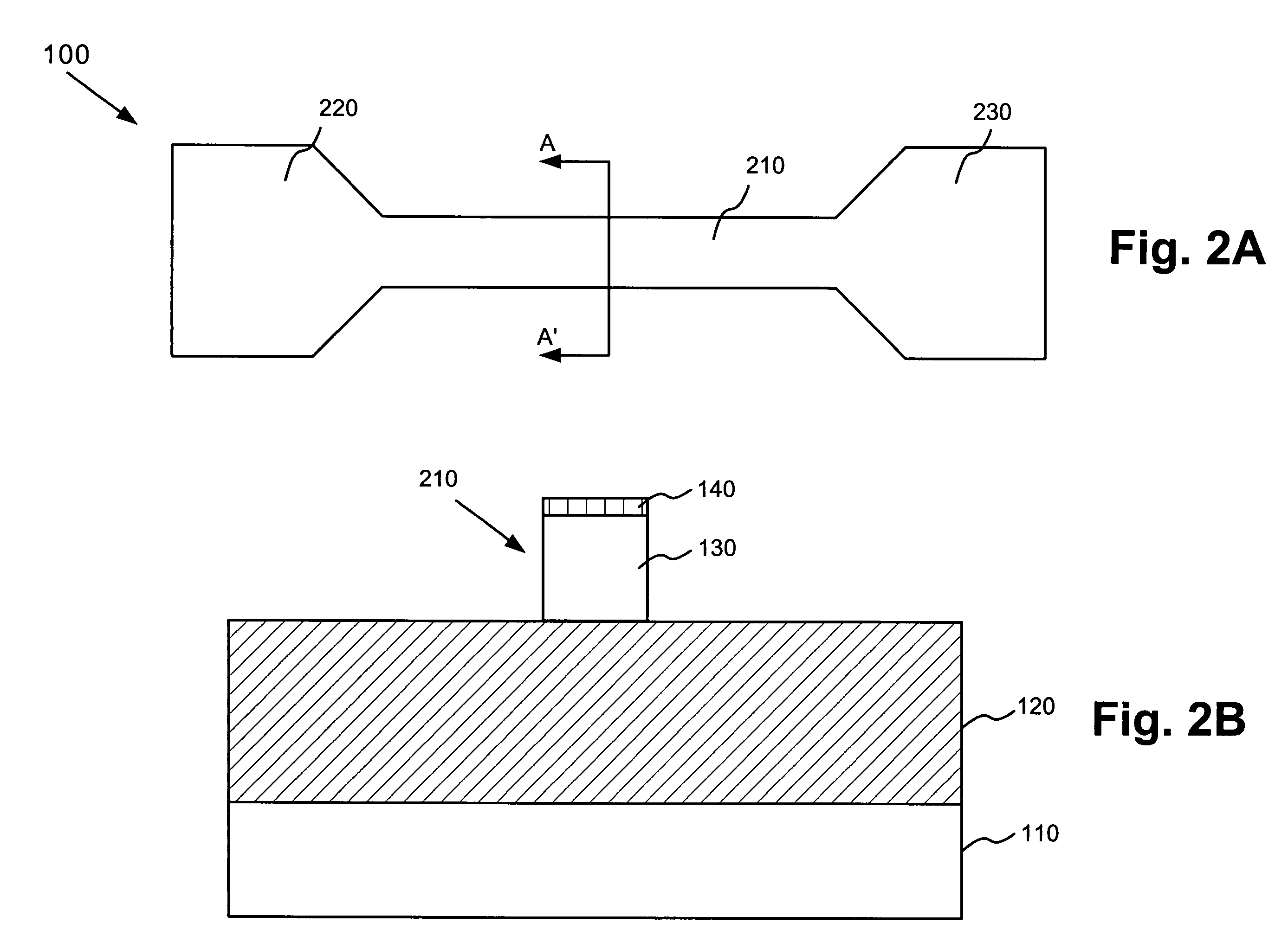
[0020]A FinFET, as the term is used herein, refers to a type of MOSFET in which a conducting channel is formed in a vertical Si “fin.”FIG. 1 illustrates the cross-section of a semiconductor device 100 formed in accordance with an embodiment of the present invention. Referring to FIG. 1, semiconductor device 100 may include a silicon on insulator (SOI) structure that includes a silicon substrate 110, a buried oxide layer 120 and a silicon layer 130 formed on the buried oxide layer 120. Buried oxide layer 120 and silicon layer 130 may be formed on substrate 110 in a conventional manner.

[0021]In an exemplary implementation, buried oxide ...


PUM


Abstract

A semiconductor device includes a semiconductor fin formed on an insulator and sidewall spacers formed adjacent the sides of the fin. A gate material layer is formed over the fin and the sidewall spacers and etched to form a gate. The presence of the sidewall spacers causes a topology of the gate material layer to smoothly transition over the fin and the first and second sidewall spacers.

Description

TECHNICAL FIELD[0001]The present invention relates to semiconductor devices and methods of manufacturing semiconductor devices. The present invention has particular applicability to double-gate devices.BACKGROUND ART[0002]The escalating demands for high density and performance associated with ultra large scale integration semiconductor devices require design features, such as gate lengths, below 100 nanometers (nm), high reliability and increased manufacturing throughput. The reduction of design features below 100 nm challenges the limitations of conventional methodology.[0003]For example, when the gate length of conventional planar metal oxide semiconductor field effect transistors (MOSFETs) is scaled below 100 nm, problems associated with short channel effects, such as excessive leakage between the source and drain, become increasingly difficult to overcome. In addition, mobility degradation and a number of process issues also make it difficult to scale conventional MOSFETs to inc...

Claims


Application Information

Patent Timeline
Patent Type & Authority Patents(United States)
IPC IPC(8): H01L27/01
CPCH01L29/42384H01L29/66795H01L29/785H01L29/4908H01L21/823431Y10S257/90
Inventor YU, BINWANG, HAIHONG
Owner ADVANCED MICRO DEVICES INC
Why Eureka
Try Eureka