Vertical bipolar transistor with a majority carrier accumulation layer as a subcollector for SOI BiCMOS with reduced buried oxide thickness for low-substrate bias operation

a bipolar transistor and accumulation layer technology, applied in the field of semiconductor devices, can solve the problems of inability to scale down (less than 30 nm) easily without more advanced and expensive lithography technologies, and the thickness subcollector of conventional bipolar junction transistors (bjts) becomes incompatible with the integration of high-performance soi cmos devices, and achieves the effect of reducing substrate bias

Inactive Publication Date: 2006-10-03
GLOBALFOUNDRIES INC
View PDF2 Cites 15 Cited by
  • Summary
  • Abstract
  • Description
  • Claims
  • Application Information

AI Technical Summary

Benefits of technology

[0008]The present invention provides a vertical SOI BJT which uses a SOI layer with a back gate-induced majority carrier accumulation layer as a subcollector located on regions of a second buried insulating region having a second thickness using a standard SOI starting wafer with a first buried insulating region having a first thickness and the method thereof. In accordance with the present invention, the first thickness of the first buried insulating region is greater than the second thickness of the second buried insulating region. The reduced thickness of the second buried insulating region underneath the bipolar devices allows for a significantly reduced substrate bias that is CMOS compatible, while maintaining the advantages of the thick first buried insulating region underneath the CMOS.
[0009]The accumulation layer can then be formed to reduce collector resistance and transit time by applying a back-bias that will not compromise the quality and reliability of the CMOS.
[0020]With such a reduced buried insulating layer thickness underneath the bipolar device, a significantly reduced substrate bias (less than 3 V) compatible with the CMOS is able to create a strong enough vertical electric field to form an accumulation layer which forms the subcollector of the inventive device, while maintaining the advantages of a thick first buried insulating layer underneath the CMOS.

Problems solved by technology

However, as complementary metal oxide semiconductor (CMOS) adopts thin silicon-on-insulator (SOI) substrates for lower power and higher speed (due to device scaling), the thick subcollector of conventional bipolar junction transistors (BJTs) becomes incompatible with the integration of high-performance SOI CMOS devices.
Even though lateral SOI BJT devices are easier to integrate with SOI CMOS, the performance of such devices is quite limited.
Hence, it cannot be scaled down (less than 30 nm) readily without more advanced and more expensive lithography technologies such as e-beam lithography.
A problem with the SOI BJT device described above is that the buried oxide (BOX) layer in high performance CMOS SOI substrates is typically 100–200 nm thick.
As a result, the substrate bias needed for significant performance improvement is unacceptably large (greater than about 20 V).

Method used


Image

  • Vertical bipolar transistor with a majority carrier accumulation layer as a subcollector for SOI BiCMOS with reduced buried oxide thickness for low-substrate bias operation
  • Vertical bipolar transistor with a majority carrier accumulation layer as a subcollector for SOI BiCMOS with reduced buried oxide thickness for low-substrate bias operation
  • Vertical bipolar transistor with a majority carrier accumulation layer as a subcollector for SOI BiCMOS with reduced buried oxide thickness for low-substrate bias operation

Examples


Embodiment Construction

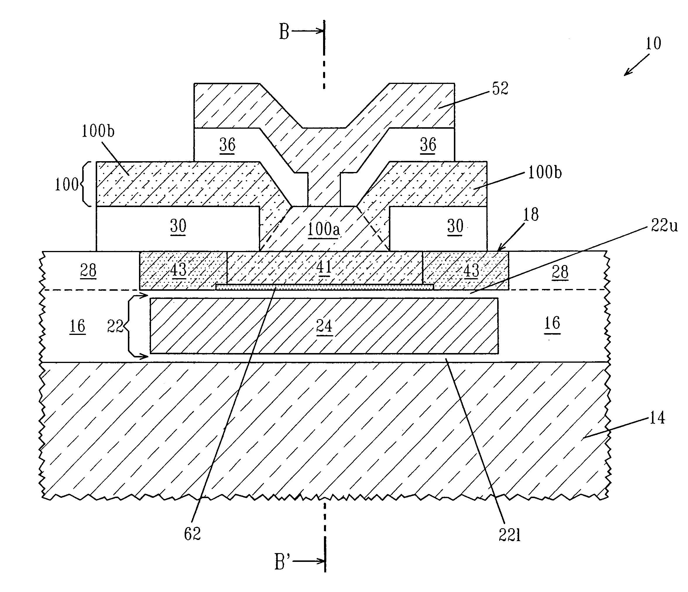
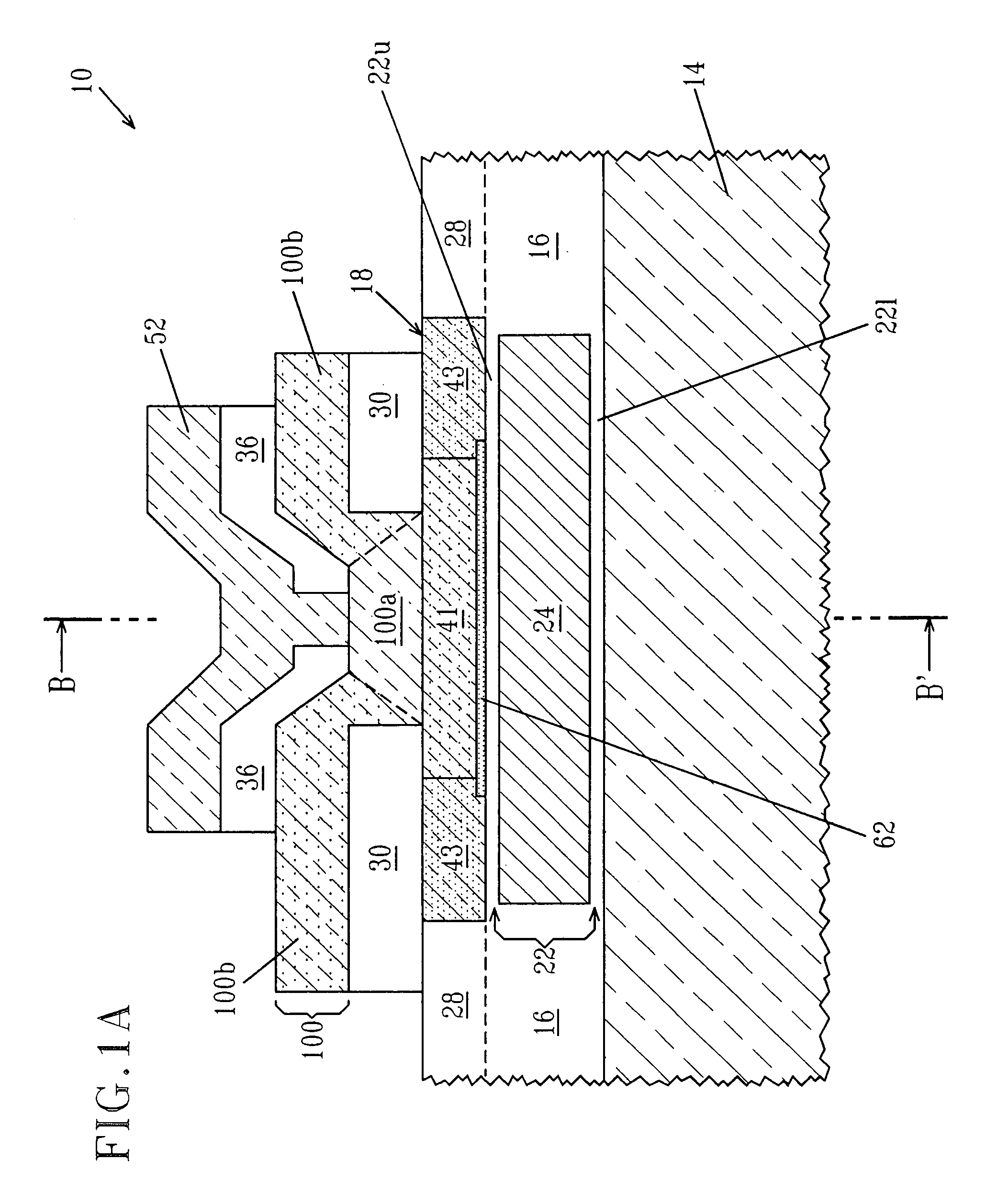
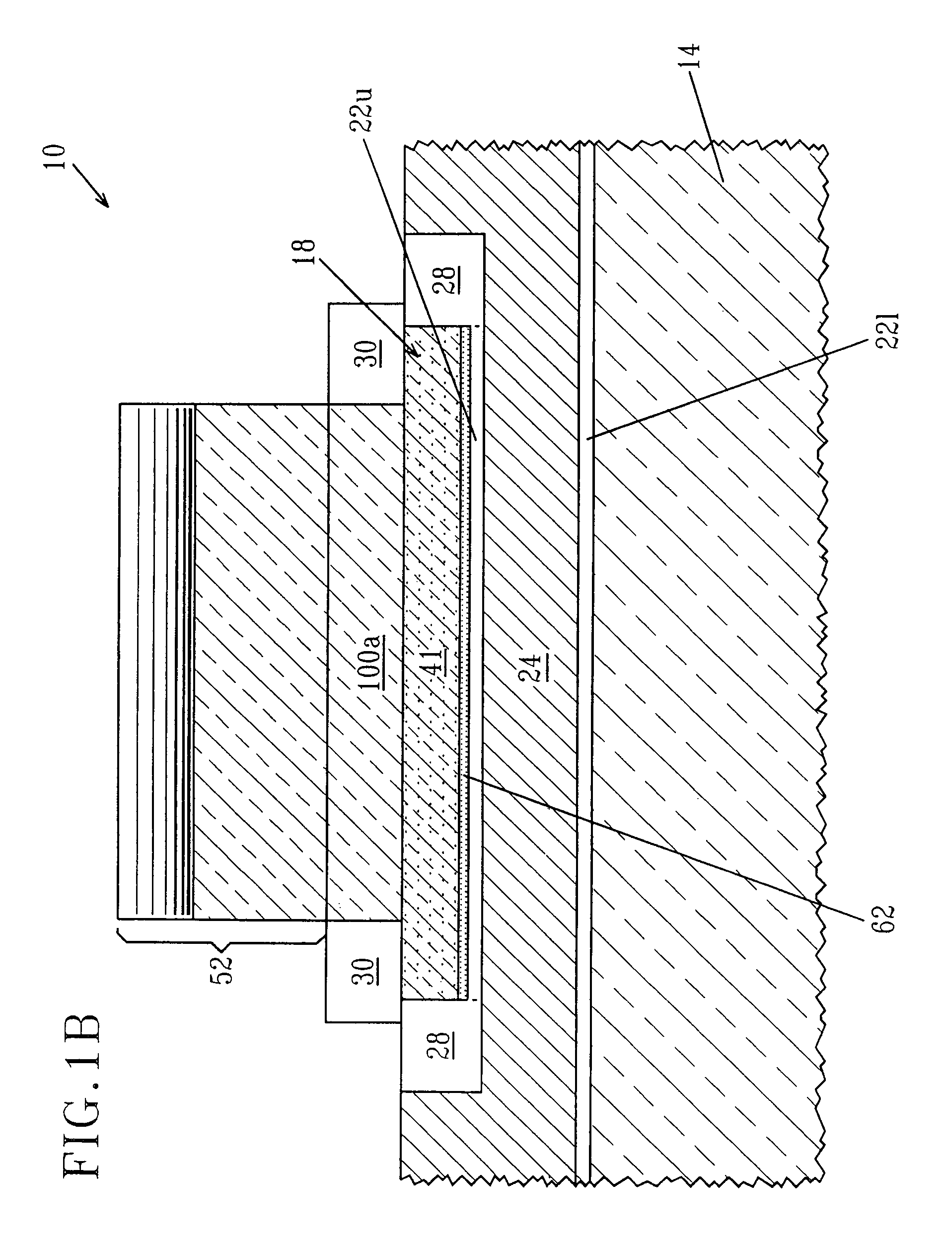
[0035]The present invention, which provides a vertical SOI BJT which uses a SOI layer with a back gate-induced accumulation layer as the subcollector located on regions of a second buried insulating region having a second thickness using a standard SOI starting wafer with a first buried insulating region having a first thickness and the method thereof, will now be described in greater detail by referring to the drawings that accompany the present application. The drawings are provided for illustrative purposes and thus they are not drawn to scale. Moreover, in the drawings like and / or corresponding elements are referred to by like reference numerals.

[0036]The present invention provides a bipolar transistor structure that includes a conductive back electrode for receiving a bias voltage, a second buried insulating layer located over the conductive back electrode, and a first semiconductor layer, which comprises an SOI layer of a SOI substrate, located over the second buried insulatin...


PUM


Abstract

The present invention provides a “subcollector-less” silicon-on-insulator (SOI) bipolar junction transistor (BJT) that has no impurity-doped subcollector. Instead, the inventive vertical SOI BJT uses a back gate-induced, majority carrier accumulation layer as the subcollector when it operates. The SOI substrate is biased such that the accumulation layer is formed at the bottom of the first semiconductor layer. The advantage of such a device is its CMOS-like process. Therefore, the integration scheme can be simplified and the manufacturing cost can be significantly reduced. The present invention also provides a method of fabricating BJTs on selected areas of a very thin BOX using a conventional SOI starting wafer with a thick BOX. The reduced BOX thickness underneath the bipolar devices allows for a significantly reduced substrate bias compatible with the CMOS to be applied while maintaining the advantages of a thick BOX underneath the CMOS. A back-gated CMOS device is also provided.

Description

FIELD OF THE INVENTION[0001]The present invention relates to a semiconductor device, and more particularly a vertical bipolar transistor that is formed using silicon-on-insulator (SOI) integrated bipolar transistor and complementary metal oxide semiconductor (hereinafter BiCMOS) technology.BACKGROUND OF THE INVENTION[0002]The semiconductor industry has been seeking more cost effective solutions for manufacturing BiCMOS devices for mass applications of radio frequency (RF) / analog and wireless / fiber-based telecommunications for decades. Si / SiGe BiCMOS technology is widely used and has been quite successful. However, as complementary metal oxide semiconductor (CMOS) adopts thin silicon-on-insulator (SOI) substrates for lower power and higher speed (due to device scaling), the thick subcollector of conventional bipolar junction transistors (BJTs) becomes incompatible with the integration of high-performance SOI CMOS devices.[0003]In order to facilitate integration with SOI CMOS, lateral...

Claims


Application Information

Patent Timeline
Patent Type & Authority Patents(United States)
IPC IPC(8): H01L29/70
CPCH01L21/84H01L27/1203H01L29/0821H01L29/66265H01L29/7317
Inventor HO, HERBERT L.KUMAR, MAHENDEROUYANG, QIQINGPAPWORTH, PAUL A.SHERAW, CHRISTOPHER D.STEIGERWALT, MICHAEL D.
Owner GLOBALFOUNDRIES INC
Why Eureka
Try Eureka