Reinforced bond pad for a semiconductor device

a technology of reinforced bonding and semiconductor devices, which is applied in the direction of semiconductor devices, semiconductor/solid-state device details, electrical apparatus, etc., can solve the problems of preventing a reliable electrical connection between the bonding pad and the packaging pin, affecting the performance of the device, and affecting the reliability of the bonding pad

Active Publication Date: 2006-10-03
BELL SEMICON LLC
View PDF3 Cites 65 Cited by
  • Summary
  • Abstract
  • Description
  • Claims
  • Application Information

AI Technical Summary

Benefits of technology

[0014]The subject invention is directed to novel support structures for pad reinforcement in conjunction with new pad designs for semiconductor devices. The new pad designs avoid the problems associated with probe testing by providing a probe region that is separate from a wire bond region. Separating the probe region from the wire bond region and forming the bond pad over active circuitry has several advantages. By separating the probe region from the wire bond region, the wire bond region is not damaged by probe testing, allowing for more reliable wire bonds. Also, forming the bond pad over active circuitry, including metal interconnect layers, allows the integrated circuit to be smaller.
[0017]In this manner, the metal-filled features in combination with the two metal layers provide a strong composite interconnect structure that distributes the stress and / or force applied during device testing and wire bonding. The support structure minimizes the amount of damage occurring to device components subjacent to the bonding pad. In addition, the isolation of the dielectric sections inhibits propagation of cracking, and ideally confines cracks within a periphery of the array of the recesses.

Problems solved by technology

The devices are subjected to thermal and mechanical stresses during electrical testing during wafer “sort” and subsequent assembly procedures.
Damage to the device may be caused during wafer sorting, when the testing probes are pressed against the bonding pad.
During the probing operation, bond pad metal may be deformed, “gouged” or “ploughed” into one or more regions of the bond pad, exposing underlying layers such as barrier materials, dielectrics and / or other conductors such as aluminum and copper, thus preventing a reliable electrical connection between the bond pad and the packaging pin during subsequent wire bonding.
Moreover, the nature of the bond may be mechanically and metallurgically weak, leading to wire lift-off or a “non-stick” (no adherence) situation.
This problem is exacerbated by the ever decreasing sizes of bond pad on which smaller wire bonds are formed, leaving very small regions where a sound wire bond is possible.
Furthermore, during the wire bond operations, device layers underlying the bond pad are compressed and in some instances materials or components may be cracked and damaged.
Dielectric cracking can occur and cracks can propagate through the layer to device components, which in turn may be damaged.
Components may also be fabricated underneath the bond pad, and may be damaged directly from the force of the probe and wire bond operations.

Method used


Image

  • Reinforced bond pad for a semiconductor device
  • Reinforced bond pad for a semiconductor device
  • Reinforced bond pad for a semiconductor device

Examples


embodiment 300

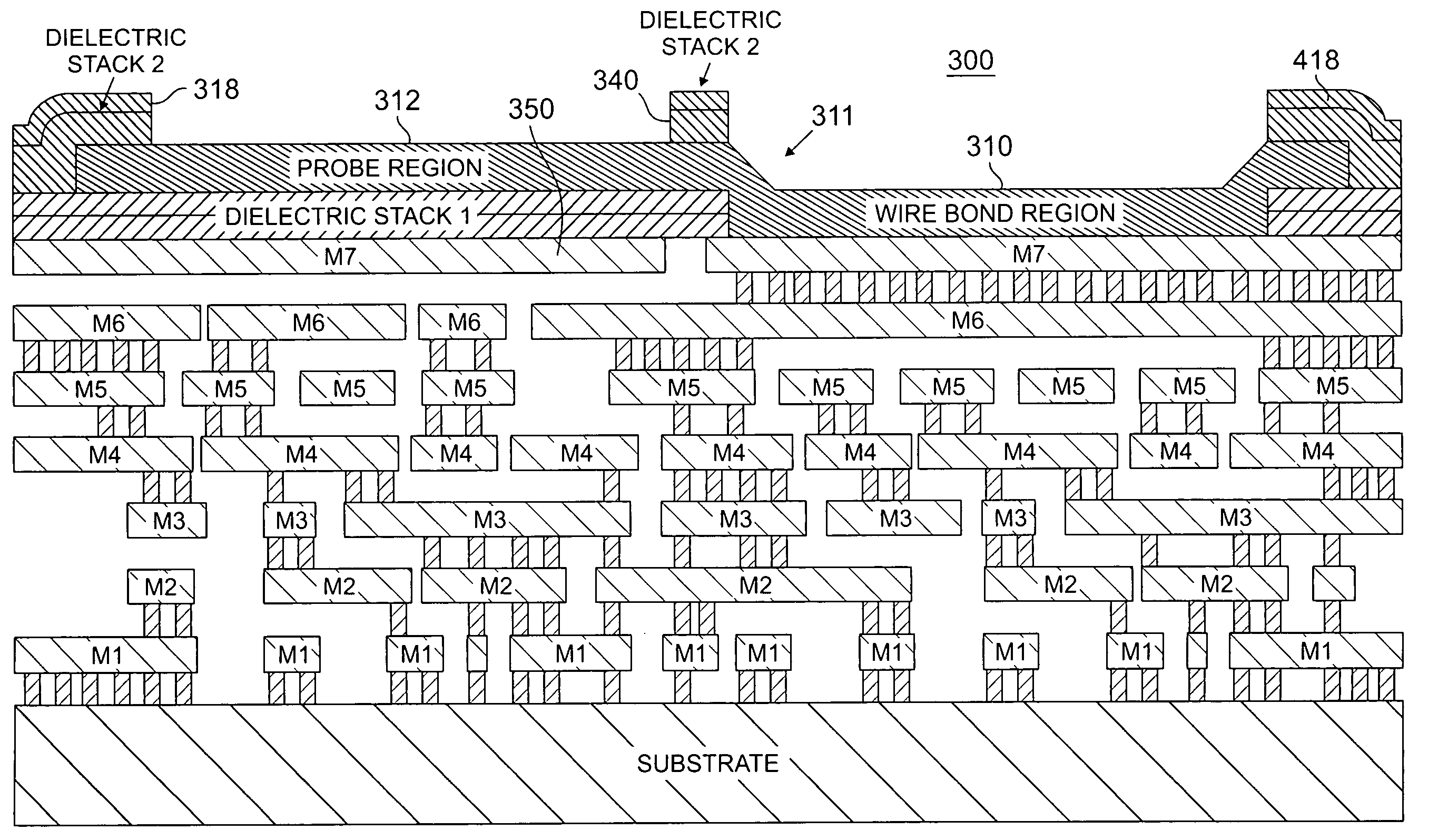
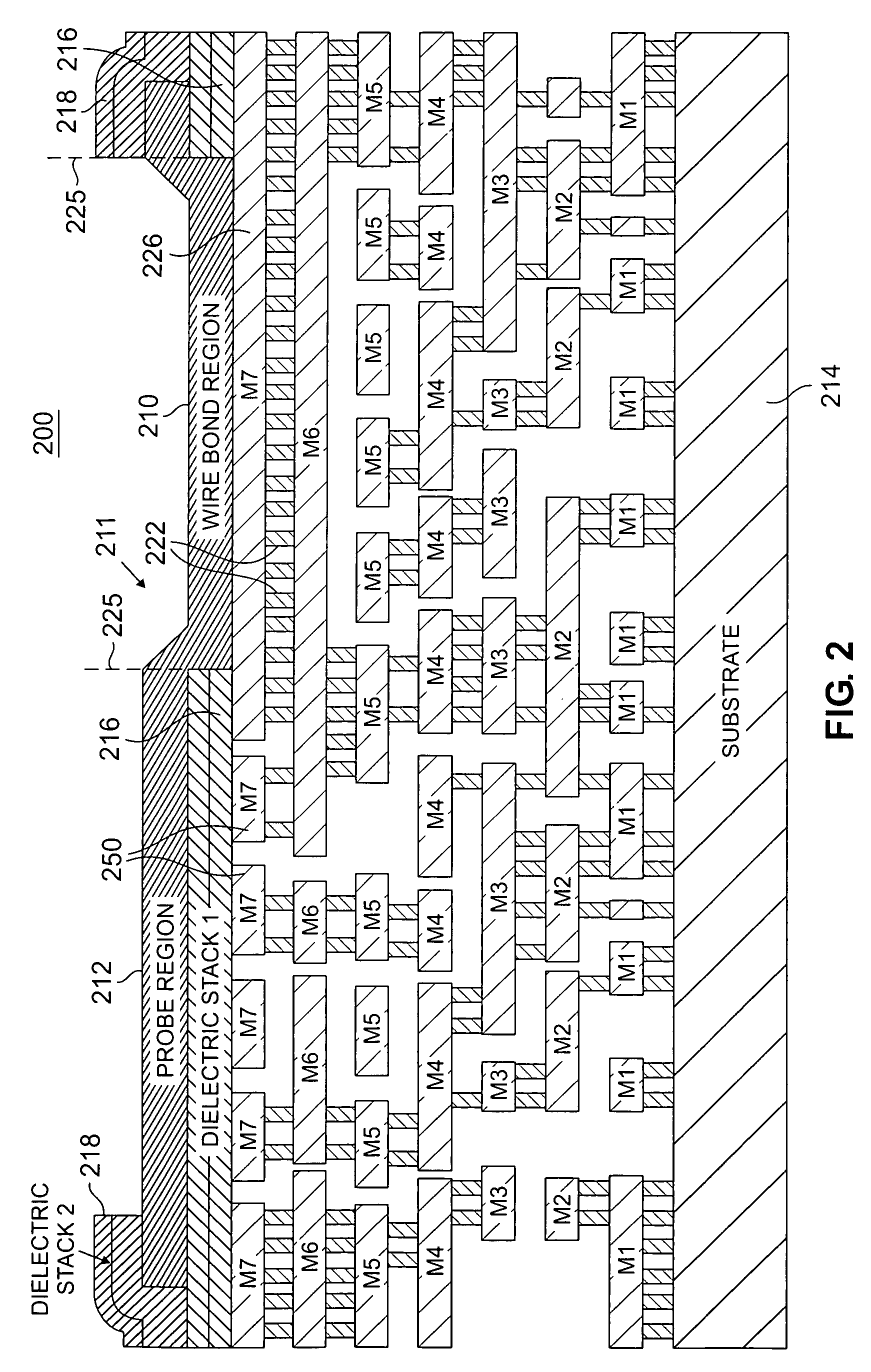
[0028]In FIG. 2, metal layers M7 and M6, insulating layer 228, and metal features 222 form what is referred to herein as a 2 / 1 support structure. This is because there are two metal layers with one intervening dielectric region between a metal support regions, such as metal filled features 222. Turning to FIG. 3, the semiconductor device embodiment 300 has a 2 / 1 support structure similar to that of device 200. However, device 300 comprises a second outer passivation layer 318 which has been patterned to provide separating region 340 positioned on top of the bond pad 311. The provision of the separating region 340 serves to prevent probe tips from flowing over into the wire bond region 310 during probe testing. In addition, device 300 comprises a floating metal region 350 positioned under the probe region 312. The floating metal region 350 is derived from M7 and may be advantageous to use since it has a different potential than a conventional connected pad, shown as 250 in FIG. 2. Th...

embodiment 500

[0030]FIG. 5 shows a semiconductor device embodiment 500 of the subject invention wherein metal layers M6, M7 and M8 for a 3 / 2 support structure, i.e., three metal layers with two metal filled features with intervening dielectric positioned between M5 and M6, M6 and M7. The bond pad has separate wire bond 510 and probe 512 regions that are separated by separating region 540 formed from second passivation layer 518. The probe region is supported by a floating metal pad 540 that is mesh patterned as described above.

embodiment 600

[0031]The semiconductor device embodiment 600 shown in FIG. 6 comprises a bond pad 611 comprising a wire bond region 610 and a probe region 612. The wire bond region 610 and probe region 612 are contiguous and coplanar, wherein the probe region 612 generally does not cover a first passivation layer 616. Separating the wire bond region 610 and the probe region 612 is a separating region 640 formed from a second passivation layer 618. The probe region 612 is generally supported by dielectric material 655 immediately subjacent to the probe region 612. The support structure subjacent to the wire bond region 610 is a 2 / 1 structure formed from metal layers M6 and M7 and intervening dielectric and metal filled features 628.

[0032]FIG. 7 shows a semiconductor device embodiment 700 similar to embodiment 600 wherein the bond pad 711 comprises a coplanar and contiguous wire bond 710 and probe 712 regions. However, device 700 comprises a 3 / 2 support structure under wire bond region 710 formed fr...


PUM


Abstract

Disclosed herein are novel support structures for pad reinforcement in conjunction with new bond pad designs for semiconductor devices. The new bond pad designs avoid the problems associated with probe testing by providing a probe region that is separate from a wire bond region. Separating the probe region 212 from the wire bond region 210 and forming the bond pad 211 over active circuitry has several advantages. By separating the probe region 212 from the wire bond region 210, the wire bond region 210 is not damaged by probe testing, allowing for more reliable wire bonds. Also, forming the bond pad 211 over active circuitry, including metal interconnect layers, allows the integrated circuit to be smaller.

Description

BACKGROUND OF THE INVENTION[0001]The present invention relates generally to the fabrication of semiconductor devices, and the packaging of semiconductor devices. More specifically, this invention pertains to bonding pads, probing pads and solder bump pads on semiconductor devices and support structures for bonding pads.[0002]Following the fabrication of the semiconductor devices on a wafer, each device (also known as a chip or die) is tested for functionality, or the wafers are “sorted”. Typically, a wafer having devices fabricated thereon is placed on a vacuum chuck. Electrical probes from a tester contact bonding pads formed on each of the devices to determine if individual devices are functional.[0003]After the wafers are sorted, the wafer is cut and the devices are separated from one another using cutting tools known to those skilled in the art. The devices are then assembled onto a substrate using procedures known as die attach or die bonding.[0004]Subsequent to the attachment ...

Claims


Application Information

Patent Timeline
Patent Type & Authority Patents(United States)
IPC IPC(8): H01L23/12H01L23/053H01L23/48H01L23/52H01L29/40
CPCH01L23/3171H01L24/48H01L24/05H01L2224/05554H01L2224/04042H01L2224/05073H01L2224/05093H01L2224/05166H01L2224/05181H01L2224/05187H01L2224/05624H01L2224/05644H01L2224/05647H01L2224/48463H01L2924/01013H01L2924/01014H01L2924/01022H01L2924/01027H01L2924/01029H01L2924/01073H01L2924/01074H01L2924/01079H01L2924/01082H01L2924/014H01L2924/04941H01L2924/04953H01L2924/05042H01L2924/14H01L2224/02166H01L2224/451H01L2224/05553H01L2924/01033H01L2924/01019H01L2924/00014H01L2224/45099H01L2924/00H01L24/45H01L24/49H01L2224/023H01L2224/49175H01L2924/00015H01L2924/0001
Inventor ANTOL, JOZE E.SEITZER, PHILIP WILLIAMCHESIRE, DANIEL PATRICKMENGEL, RAFE CARLARCHER, VANCE DOLVANGANS, THOMAS B.KOOK, TAEHOMERCHANT, SAILESH M.
Owner BELL SEMICON LLC
Why Eureka
Try Eureka