

Method of sealing two plates with the formation of an ohmic contact therebetween
a technology of ohmic contact and sealing process, which is applied in the manufacturing of semiconductor/solid-state devices, basic electric elements, electrical equipment, etc., can solve the problems of complex sealing, difficult to bond metallic layers, and additional technological steps
- Summary
- Abstract
- Description
- Claims
- Application Information
AI Technical Summary
Benefits of technology
Problems solved by technology
Method used
Image

Examples
example 1
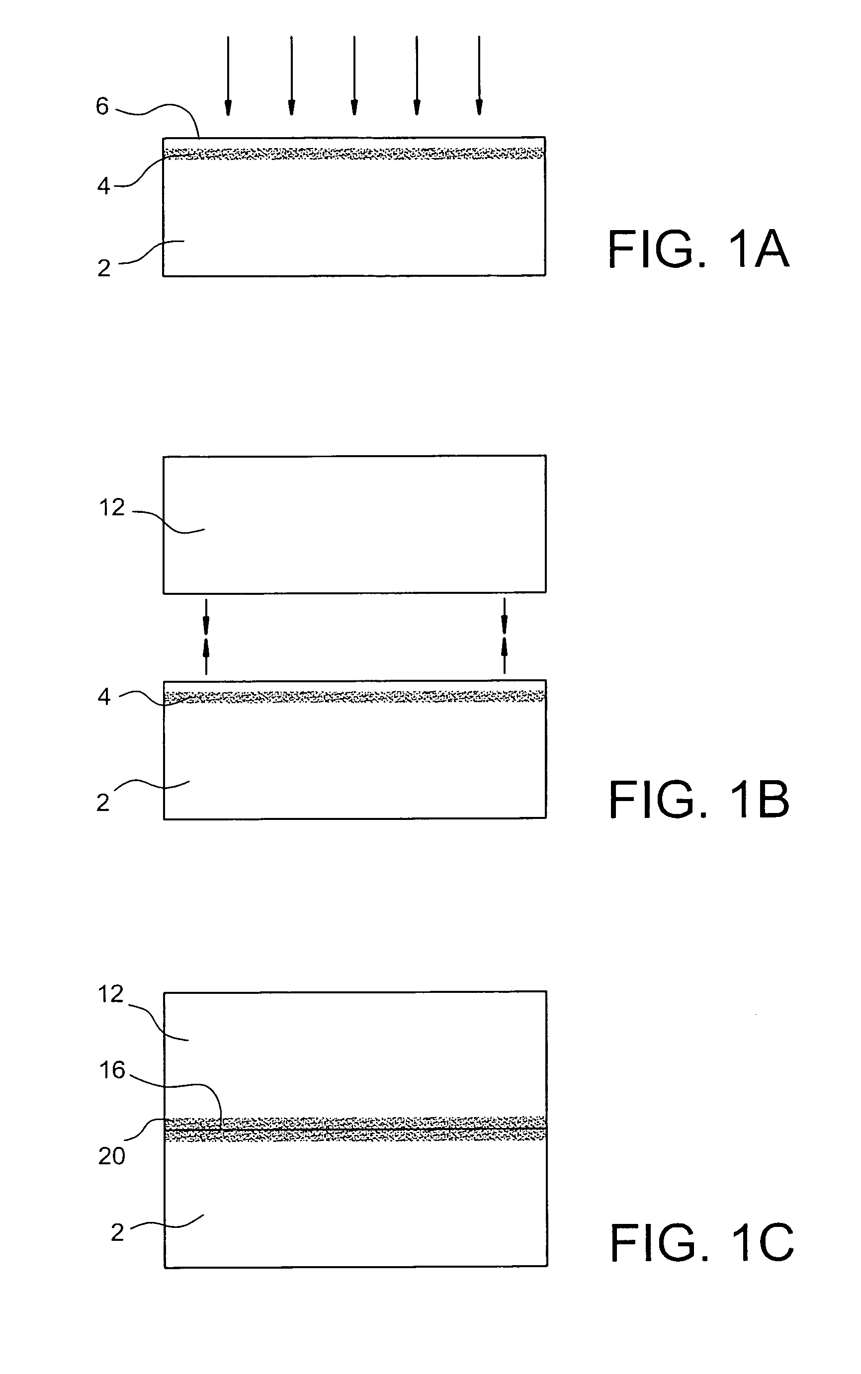
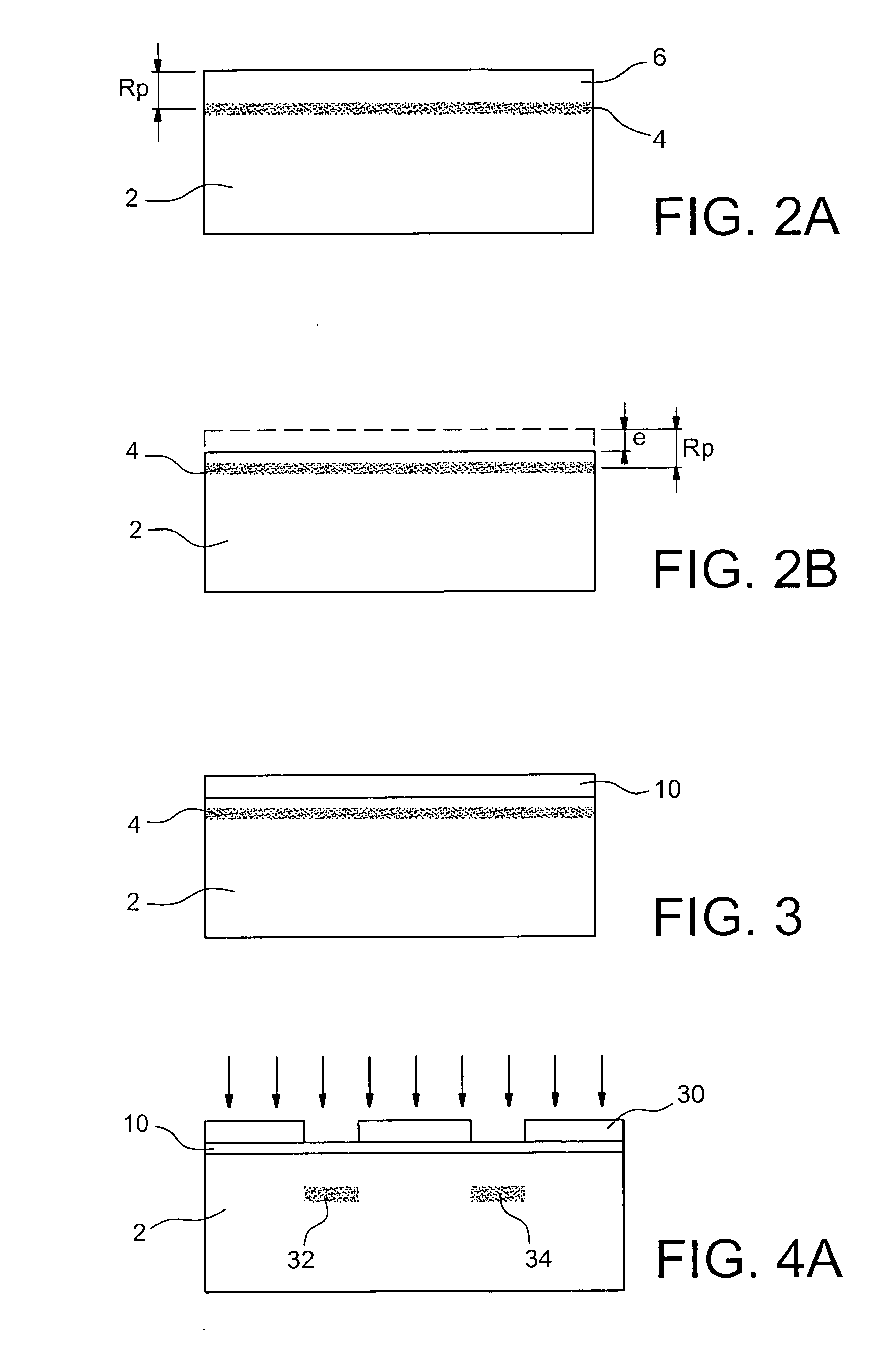
[0055] Ni+ ions are implanted in a silicon wafer 2 covered by a film 10 of silicon oxide (FIG. 3) with a thickness of 5 nm, at a dose of 2×10¹⁷ ions / cm2 and an energy of 10 keV. According to the SRIM-2000 simulation software, the implantation Rp is located at a depth of about 12 nm and about 7 nm from the silicon surface. After implantation, the silicon oxide 10 is withdrawn and a second wafer 12 made of implanted or non-implanted silicon (FIG. 1B) is bonded directly. A siliciding annealing is done at about 300° C. to form the Ni2Si silicide 20, that will form up to and beyond the bonding interface 16 (FIG. 1C).
[0056] In one variant of this example, an intermediate layer (for example amorphous silicide) could be deposited on the implanted substrate after implantation. The thickness of this layer will be chosen to be compatible with the formation of the alloy at the bonding interface. If necessary, this intermediate layer could then be thinned before bonding. For example, this layer...
example 2
[0057] Ni+ ions are implanted directly in a silicon wafer 2 at a dose of 3×10¹⁷ ions / cm2 and at an energy of 10 keV (FIG. 2A). According to the SRIM-2000 simulation software, the implantation Rp is at a depth of about 13 nm. The silicon is etched to bring the implantation Rp close to the surface, for example with an SC1 type chemical solution (see above) until the implantation RP is close to the surface (FIG. 2B), for example at a depth of the order of 5 nm. A second wafer 12 made of silicon is then bonded directly (FIG. 1B). The next step is a siliciding annealing at about 300° C. so as to form an Ni2Si silicide that will then be formed up to and beyond the bonding interface 16 (FIG. 1C).
[0058] A variant of this example consists of making all or part of the surface layer of the substrate 2 amorphous. Amorphisation of the material (in this case silicon) will facilitate diffusion of the implanted species in this material. If the amorphous material is present on the surface, diffusio...
example 3
[0059] One variant of example 2 consists of implanting the Ni+ species at a dose of 2×10¹⁷ ions / cm2 and an energy of 10 keV. According to the SRIM-2000 simulation software, the implantation Rp is at a depth of about 13 nm. The silicon is etched, for example with an SC1 type chemical solution, until the implantation RP is close to the interface (FIG. 2B), so as to bring the implantation Rp close to the surface. The next step is an argon plasma treatment before bonding to reinforce the molecular bonding energy at low temperature. Once bonded, the structure is annealed at the temperature at which the silicide is formed so as to form the Ni2Si silicide, which will be formed up to and beyond the bonding interface (FIG. 1C).
PUM
 Abstract
Description
Claims
Application Information