MOS devices with reduced recess on substrate surface

a technology of metal oxides and mos, which is applied in the direction of semiconductor devices, electrical equipment, transistors, etc., can solve the problems of difficult to achieve a depth of only 30 , more prone to diffusion of impurities in the sige, so as to improve the short channel effect, reduce the junction depth of the mos device, and increase the drive current of the device

Active Publication Date: 2007-02-15
TAIWAN SEMICON MFG CO LTD
View PDF6 Cites 73 Cited by
  • Summary
  • Abstract
  • Description
  • Claims
  • Application Information

AI Technical Summary

Benefits of technology

[0015] With the depth of the recesses in the substrate reduced, the junction depth of the MOS d

Problems solved by technology

The scaling of VLSI circuits is a constant effort.
In prior art pMOS devices, if the hard mask is removed by H3PO4 after epitaxially growing SiGe regions 2, the depth Dp of the recesses 12 is easily greater than about 30 Å, and even achieving a depth of only 30 Å is difficult.
When doped SiGe regions are formed in pMOS

Method used


Image

  • MOS devices with reduced recess on substrate surface
  • MOS devices with reduced recess on substrate surface
  • MOS devices with reduced recess on substrate surface

Examples


Embodiment Construction

[0021] The making and using of the presently preferred embodiments are discussed in detail below. It should be appreciated, however, that the present invention provides many applicable inventive concepts that can be embodied in a wide variety of specific contexts. The specific embodiments discussed are merely illustrative of specific ways to make and use the invention, and do not limit the scope of the invention.

[0022] The intermediate stages of manufacturing a preferred embodiment of the present invention are illustrated in FIGS. 4 through 16. Throughout the various views and illustrative embodiments of the present invention, like reference numbers are used to designate like elements.

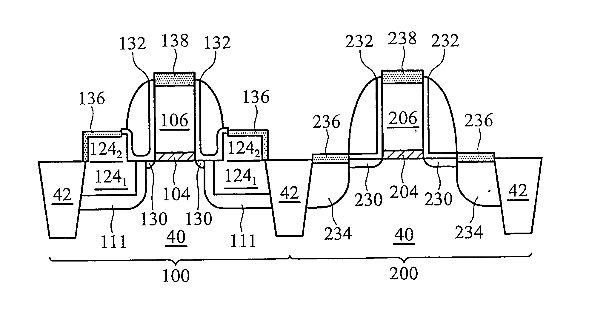
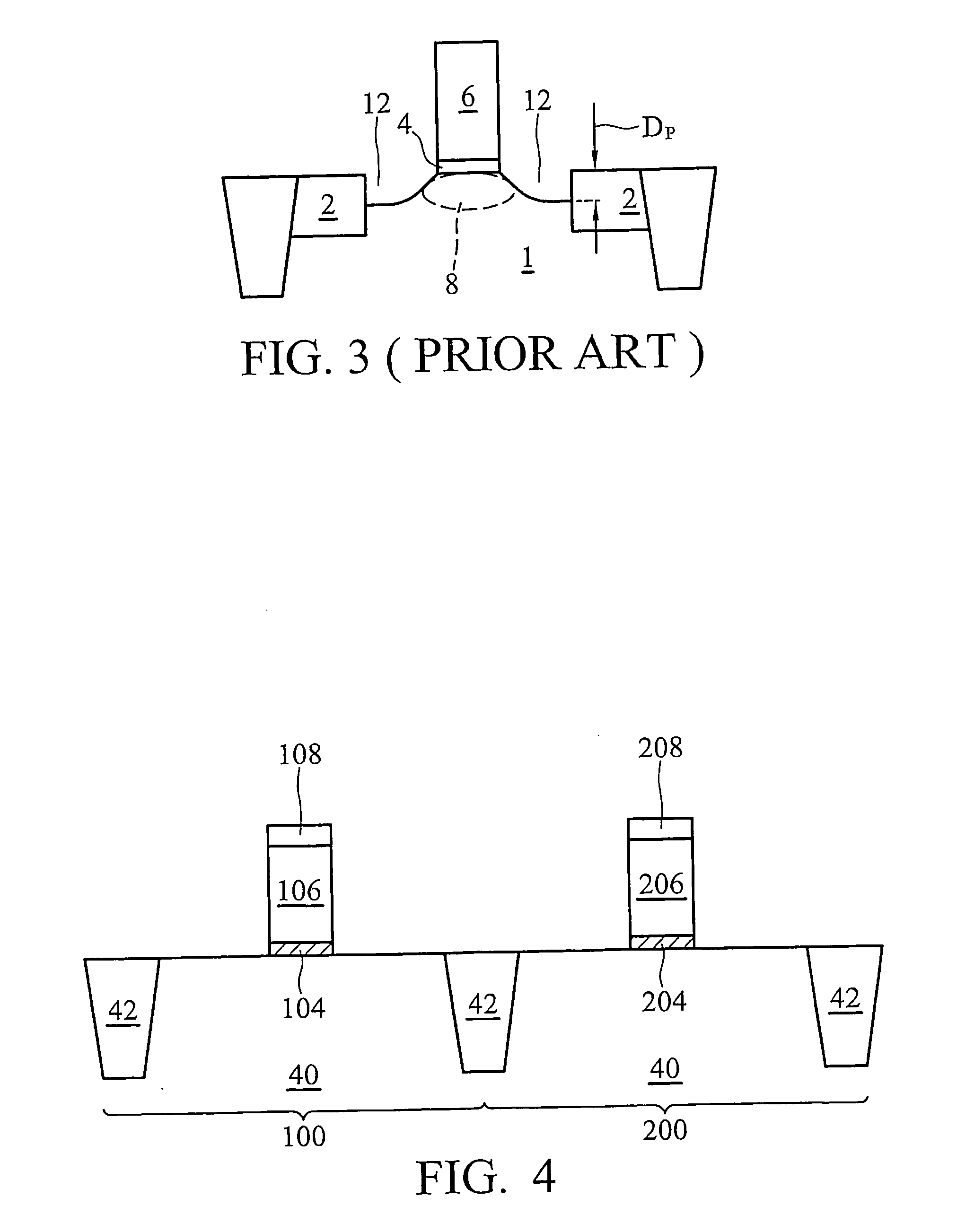
[0023]FIG. 4 illustrates two gate stacks formed on a substrate 40, which comprises two regions, a region 100 for forming a pMOS device and a region 200 for forming an nMOS device. The regions 100 and 200 are isolated by shallow trench isolations 42. The gate stack in the pMOS region 100 includes a ga...


PUM


Abstract

A MOS device having reduced recesses under a gate spacer and a method for forming the same are provided. The MOS device includes a gate structure overlying the substrate, a sidewall spacer on a sidewall of the gate structure, a recessed region having a recess depth of substantially less than about 30 Å underlying the sidewall spacer, and a silicon alloy region having at least a portion in the substrate and adjacent the recessed region. The silicon alloy region has a thickness of substantially greater than about 30 nm. A shallow recess region is achieved by protecting the substrate when a hard mask on the gate structure is removed. The MOS device is preferably a pMOS device.

Description

[0001] This application claims priority to provisional patent application ser. no. 60 / 707,084, filed on Aug. 10, 2005, entitled “Scalable High Performance MOSFETs with High Strain,” which application is hereby incorporated herein by reference.TECHNICAL FIELD [0002] This invention relates generally to semiconductor devices, and more particularly to metal-oxide-semiconductor (MOS) devices, and even more particularly to the structure and fabrication methods of MOS devices having highly-stressed channel regions. BACKGROUND [0003] The scaling of VLSI circuits is a constant effort. With circuits become smaller and faster, improvement of device driving current becomes more important. Metal-oxide-semiconductor (MOS) transistor current is closely related to gate length, gate capacitance, and carrier mobility in the channel region. Shortening poly-gate length, increasing gate capacitance and increasing carrier mobility can improve the device currents of MOS devices. Gate length reduction is a...

Claims


Application Information

Patent Timeline
IPC IPC(8): H01L29/768
CPCH01L21/823807H01L21/823814H01L21/823864H01L29/165H01L29/66507H01L29/6653H01L29/7848H01L29/6656H01L29/6659H01L29/66628H01L29/7833H01L29/7834H01L29/66545
Inventor WANG, CHIH-HAOWANG, TA-WEI
Owner TAIWAN SEMICON MFG CO LTD
Why Eureka
Try Eureka